Processing device with scrap iron cleaning function for semiconductor processing

A processing device and semiconductor technology, applied in the direction of manufacturing tools, metal processing equipment, metal processing machinery parts, etc., can solve the problems of affecting production quality, small iron filings, cumbersome operation, etc., and achieve the effect of facilitating weaving and transportation

Active Publication Date: 2022-03-08
智研信息科技(临沂)有限公司
View PDF17 Cites 1 Cited by
  • Summary
  • Abstract
  • Description
  • Claims
  • Application Information

AI Technical Summary

Problems solved by technology

[0003] When semiconductors are weaving, it is inevitable that some iron filings will be generated. If the iron filings fall onto the semiconductor device in the transport tank, it will affect its production quality, and it will easily cause the device to freeze. After adsorption, it needs to be manually peeled off from the magnetic plate. The iron filings are small, and the peeling is troublesome. The magnetic plate needs to be repeatedly disassembled and installed on the device before and after peeling, and the operation is cumbersome.

Method used


Image

  • Processing device with scrap iron cleaning function for semiconductor processing
  • Processing device with scrap iron cleaning function for semiconductor processing
  • Processing device with scrap iron cleaning function for semiconductor processing

Examples


Embodiment Construction

[0026]In order to make the technical means, creative features, goals and effects achieved by the present invention easy to understand, the present invention will be further described below in conjunction with specific embodiments.

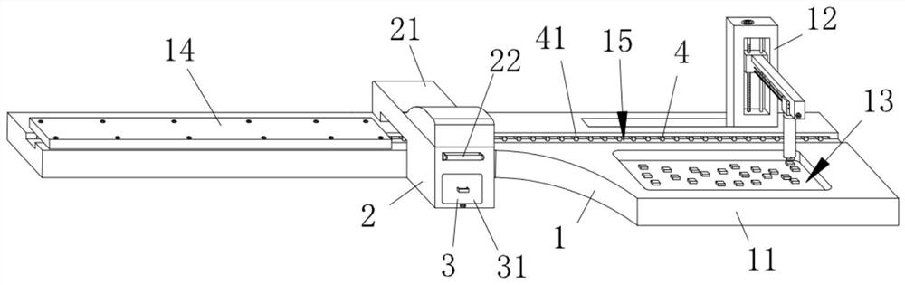
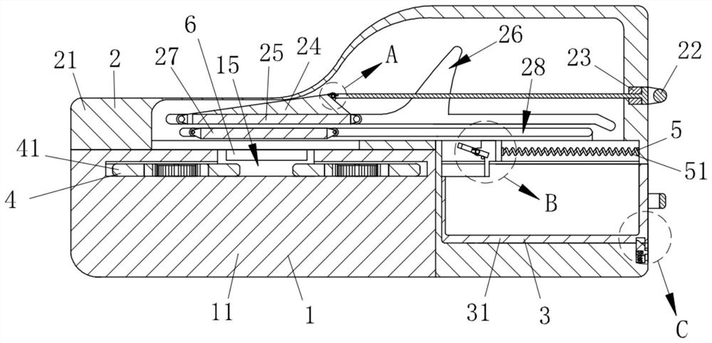
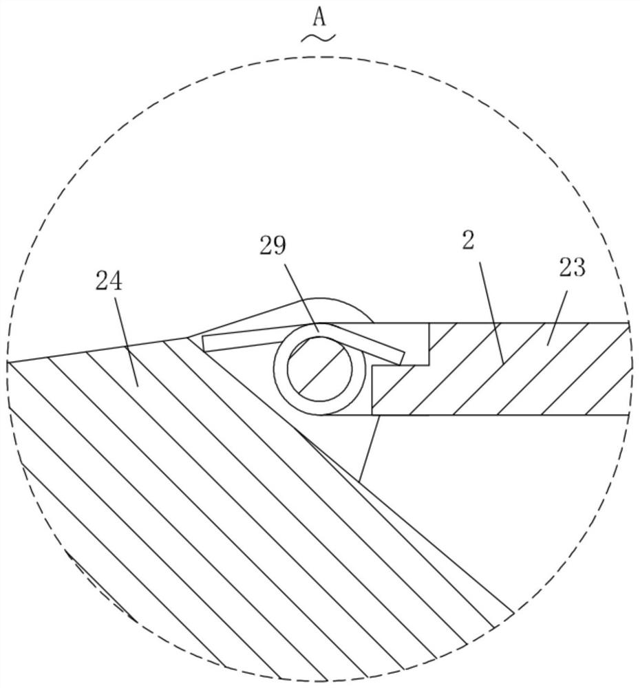
[0027] Such as Figure 1-Figure 8 As shown, the processing device for semiconductor processing according to the present invention has the function of cleaning iron filings, including a braided structure 1, the braided structure 1 is connected with a transport structure 4 for transporting semiconductor devices, and the braided structure 1 is connected with a A cleaning structure 2 for removing iron filings on the transport structure 4, the cleaning structure 2 is connected with a collection structure 3 for collecting iron filings on the cleaning structure 2, and the cleaning structure 2 is connected with a cleaning structure 2 A scraping structure 5 for scraping and cleaning, the cleaning structure 2 is equipped with an actuating structure 6 for cle...


PUM


Abstract

The invention relates to the technical field of semiconductor processing, in particular to a processing device with a scrap iron cleaning function for semiconductor processing, which comprises a weaving structure, the weaving structure is connected with a transportation structure for transporting semiconductor devices, and the weaving structure is connected with a cleaning structure for cleaning scrap iron on the transportation structure. The cleaning structure is connected with a collecting structure, the cleaning structure is connected with a scraping structure, and the cleaning structure is provided with a touch structure for cleaning scrap iron on the surface of the semiconductor device; the semiconductor device can be automatically corrected through the braiding structure, the semiconductor device can be rapidly transported, braided and processed conveniently through the transporting structure, scrap iron falling on the braiding structure can be cleaned through the cleaning structure, and the scrap iron is collected in a centralized mode through the collecting structure. The scrap iron on the cleaning structure can be better and rapidly cleaned through the scraping structure, and the scrap iron on the conveying structure can be separated from the weaving structure through the touch structure.

Description

technical field [0001] The invention relates to the technical field of semiconductor processing, in particular to a processing device for semiconductor processing with the function of cleaning iron filings. Background technique [0002] Semiconductor refers to the material whose conductivity is between conductor and insulator at normal temperature. Semiconductor is widely used in radio, television and temperature measurement. In the process of semiconductor processing, semiconductor needs to be woven and packaged. To clean up the iron filings, it is necessary to use a processing device with the function of iron filings cleaning for semiconductor processing. [0003] When semiconductors are weaving, it is inevitable that some iron filings will be generated. If the iron filings fall onto the semiconductor device in the transport tank, it will affect its production quality, and it will easily cause the device to freeze. After adsorption, it needs to be manually peeled off from...

Claims


Application Information

Patent Timeline
IPC IPC(8): B23Q11/00
CPCB23Q11/0042
Inventor 于富强闵祥峰滕兆伟冯立国马强
Owner 智研信息科技(临沂)有限公司
Why Eureka
Try Eureka