Semiconductor structure and forming method thereof
A semiconductor and patterning technology, used in semiconductor devices, semiconductor/solid-state device manufacturing, transistors, etc., can solve problems such as poor device performance, and achieve the effect of improving uniformity and performance
- Summary
- Abstract
- Description
- Claims
- Application Information
AI Technical Summary
Problems solved by technology
Method used
Image

Examples
Embodiment Construction
[0020] Currently formed devices still suffer from poor performance. The reasons for the poor performance of the device are analyzed in conjunction with a method of forming a semiconductor structure.
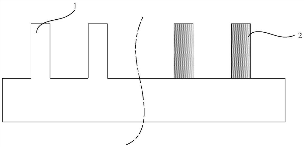
[0021] refer to figure 1 , shows a schematic structural diagram of a semiconductor structure, including a first fin 1 and a second fin 2, wherein the materials of the first fin 1 and the second fin 2 are different. Usually, in the semiconductor formation process, the first fin 1 and the second fin 2 are formed at the same time, that is, the same patterning process is used, and the first fin and the second fin are formed by dry etching at the same time.
[0022] Traditionally, it is generally believed that the first fin and the second fin formed by the same patterning process have the same size, so little attention has been paid to the problem of size uniformity that may occur in this process.
[0023] However, the inventors of the present invention have found that in the proces...
PUM
 Abstract
Description
Claims
Application Information
PatSnap Eureka turns technology decisions into work you can execute. Powered by our Innovation Knowledge Graph, it runs expert workflows across engineering, life sciences, materials and intellectual property. Get your review-ready output in minutes.


