PCB flatness measuring method and measuring device

A measurement method and flatness technology, applied in the field of PCB flatness measurement methods and measurement devices, can solve the problems of fuzzy qualitative judgment, missed judgment, and high efficiency of manual measurement, so as to improve the measurement accuracy and overcome misjudgment or missed judgment. Effect

Pending Publication Date: 2022-03-15
HUIZHOU GAOSHENGDA TECH CO LTD
View PDF10 Cites 2 Cited by
  • Summary
  • Abstract
  • Description
  • Claims
  • Application Information

AI Technical Summary

Problems solved by technology

[0003] A method for testing the flatness of PCB boards is provided in the related art. The PCB board to be tested is placed on a standard horizontal platform, and the warpage of the PCB board is detected through the naked eye observation of the inspector. However, This manual observation method usually finds the U-shaped warpage of the PCB board, but cannot find the wavy unevenness of the PCB board, and can only make a relatively vague qualitative judgment, and cannot quantitatively judge the flatness of the PCB board.
Moreover, the efficiency of manual measurement is high, and there are subjective misjudgments and missed judgments, and the measurement accuracy is not high

Method used


Image

  • PCB flatness measuring method and measuring device
  • PCB flatness measuring method and measuring device
  • PCB flatness measuring method and measuring device

Examples


Embodiment 1

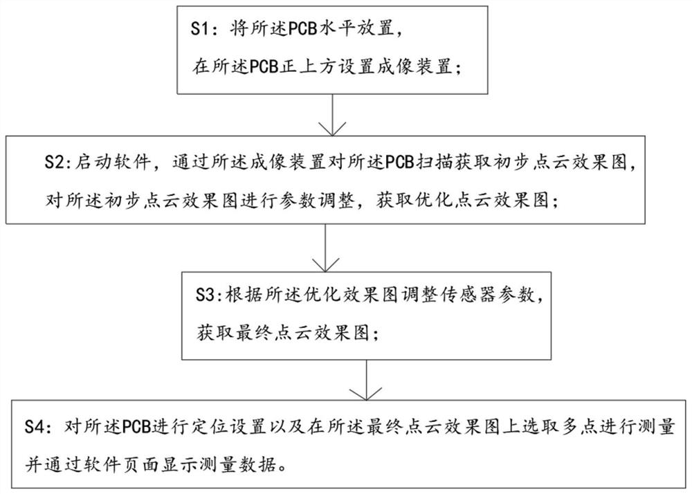
[0046] A method for measuring PCB flatness, comprising the following steps:

[0047] The following steps are described in combination with software operation.

[0048] Such as figure 1 As shown, the first step is to place the PCB-3 horizontally, and set the imaging device directly above the PCB-3. The imaging device is located at 140mm±10mm directly above the PCB-3, and the optimal height distance is 140mm. The distance between the bottom and the surface of PCB-3, the imaging device is 3D camera-1.

[0049]The second step is to start the software and scan the PCB-3 through the imaging device to obtain the preliminary point cloud rendering. The specific operation is to operate the measurement software, click Settings, switch to the setting interface, open the hardware parameter list, and open the "2D preview function". Use the imaging device to preview the planar image of PCB-3, adjust the position of PCB-3 according to the planar image preview, so that PCB-3 is located in th...

Embodiment 2

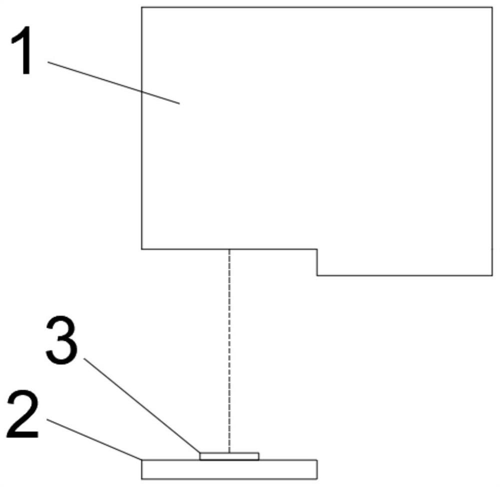
[0069] A measuring device includes: a placing platform, an imaging device and an industrial computer.

[0070] Placement platform-2: for placing the PCB-3 horizontally and fixing the imaging device directly above the PCB-3;

[0071] Imaging device: used to scan the PCB-3 and provide scanning images for the measurement software; the imaging device is provided with a lifting support, and the lower end of the lifting support is installed around the placement platform-2.


PUM


Abstract

The invention relates to the technical field of PCB detection, in particular to a PCB flatness measuring method and device, and the method comprises the steps: horizontally placing a PCB, arranging a 3D camera right above the PCB, scanning the PCB below through the 3D camera to obtain a point cloud image, carrying out the parameter adjustment of the scanned image to cut off a flying spot or a noisy spot of the image, and carrying out the measurement of the flatness of the PCB. Multi-point measurement is carried out on the surface of a PCB through a measurement operator, the PCB is positioned through the measurement operator so as to ensure that the measurement positions of the PCB are consistent, the invention provides a measurement device for detecting the flatness of the PCB, and the measurement device comprises a placement platform for placing the PCB, an imaging device for scanning the surface of the PCB and an industrial computer with built-in analysis processing software. Multi-point comprehensive measurement is selected for the surface of the PCB, and the measurement accuracy and the measurement efficiency are improved.

Description

technical field [0001] The invention relates to the technical field of PCB detection, in particular to a PCB flatness measurement method and a measurement device. Background technique [0002] With the continuous development of the circuit board industry, the electronic components mounted on high-end handheld electronic consumer products are getting smaller and smaller, and the requirements for the flatness of the circuit board surface during the mounting process are getting higher and higher. [0003] A method for testing the flatness of PCB boards is provided in the related art. The PCB board to be tested is placed on a standard horizontal platform, and the warpage of the PCB board is detected through the naked eye observation of the inspector. However, This manual observation method usually finds the U-shaped warpage of the PCB board, but cannot find the wavy unevenness of the PCB board, and can only make a relatively vague qualitative judgment, and cannot quantitatively ...

Claims


Application Information

Patent Timeline
Patent Type & Authority Applications(China)
IPC IPC(8): G01B11/30G01N21/956
CPCG01B11/30G01N21/956G01N2021/95661
Inventor 李福斌
Owner HUIZHOU GAOSHENGDA TECH CO LTD
Why Eureka
Try Eureka