PCB and manufacturing method thereof

A production method and surface fabrication technology, applied in the direction of electrical connection of printed components, structural connection of printed circuits, printed circuit components, etc., can solve the problems of tight wiring area on the surface of the PCB substrate, and improve the wiring density or component patch density. , the effect of expanding the available space

Pending Publication Date: 2022-03-15
DONGGUAN SHENGYI ELECTRONICS
View PDF4 Cites 1 Cited by
  • Summary
  • Abstract
  • Description
  • Claims
  • Application Information

AI Technical Summary

Problems solved by technology

[0003] The purpose of the present invention is to provide a PCB and its manufacturing method to solve the problem that the wiring area on the surface of the existing PCB substrate is becoming more and more tense

Method used


Image

  • PCB and manufacturing method thereof
  • PCB and manufacturing method thereof

Examples


Embodiment Construction

[0031] In order to make the purpose, features and advantages of the present invention more obvious and understandable, the technical solutions in the embodiments of the present invention will be clearly and completely described below in conjunction with the accompanying drawings in the embodiments of the present invention. Obviously, the following The described embodiments are only some, not all, embodiments of the present invention. Based on the embodiments of the present invention, all other embodiments obtained by persons of ordinary skill in the art without making creative efforts belong to the protection scope of the present invention.

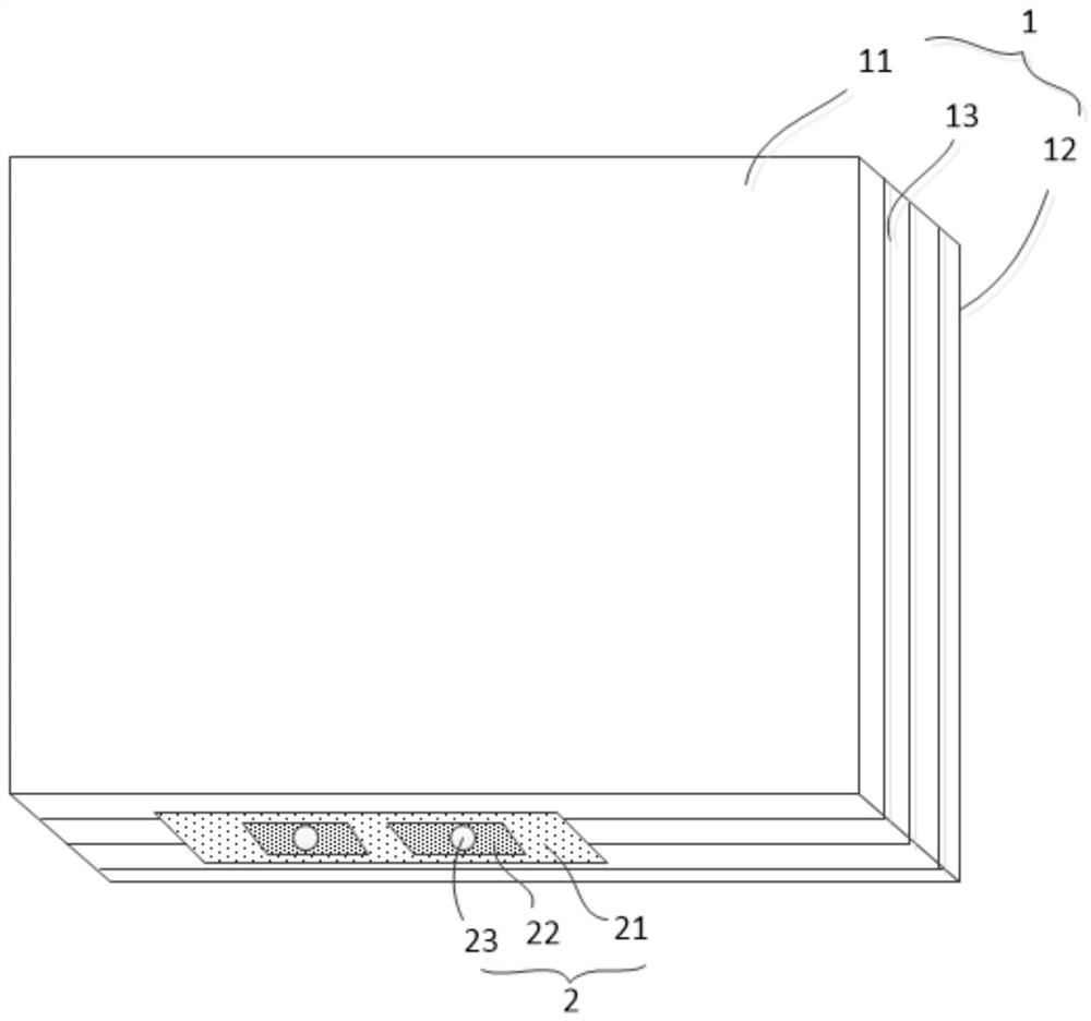
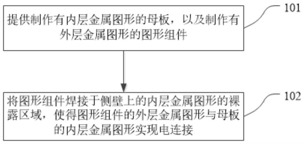
[0032] see figure 1 , the embodiment of the present invention provides a PCB, including: a motherboard 1 with at least one inner metal pattern, and a graphic component 2 with an outer metal pattern 22;

[0033] The motherboard 1 includes a top wall 11, a bottom wall 12, and a side wall 13 enclosed between the top wall 11 and the bottom w...


PUM


Abstract

The invention relates to the technical field of PCBs, and discloses a PCB and a manufacturing method thereof, and the PCB comprises a mother board provided with at least one inner-layer metal pattern, and a pattern assembly provided with an outer-layer metal pattern. The mother board comprises a top wall, a bottom wall and a side wall arranged between the top wall and the bottom wall in a surrounding mode, and the inner layer metal pattern part is exposed out of the side wall; and the pattern assembly is welded on the exposed area of the inner layer metal pattern on the side wall, so that the outer layer metal pattern of the pattern assembly is electrically connected with the inner layer metal pattern of the mother board. According to the PCB provided by the invention, the space of the side wall of the mother board is utilized, the pattern assembly with the outer-layer metal pattern is arranged on the side wall, and the pattern assembly is electrically connected with the inner-layer metal pattern of the mother board, so that the signal transmission function of the pattern assembly is realized. According to the PCB, the limited space is effectively expanded, the available space is expanded, and the wiring density or the element patch density is improved, so that the PCB meets the increasingly miniaturized and high-density development trend.

Description

technical field [0001] The present invention relates to the technical field of PCB (Printed Circuit Board, printed circuit board), in particular to a PCB and a manufacturing method thereof. Background technique [0002] In printed circuit boards, the pads are mainly divided into pin pads and surface mount pads. The pin pads have solder holes and are mainly used for soldering pin components, while the surface mount pads have no solder holes and are mainly used for surface mounting. paste components. With the miniaturization of semiconductor design, the density of components on the corresponding PCB substrate is getting higher and higher, and the pad setting area on the surface of traditional PCB is becoming more and more tense. Therefore, how to increase the mounting area of ​​PCB to meet the needs of terminal electronic products The miniaturization and high-density design requirements are urgent problems to be solved at present. Contents of the invention [0003] The obj...

Claims


Application Information

Patent Timeline
Patent Type & Authority Applications(China)
IPC IPC(8): H05K1/14H05K1/11H05K3/36
CPCH05K1/145H05K1/111H05K3/36
Inventor 陈长平王小平刘潭武袁继旺杜红兵
Owner DONGGUAN SHENGYI ELECTRONICS
Why Eureka
Try Eureka