Silicon wafer feeding and discharging system

A silicon wafer and blanking technology, applied in the fields of photovoltaic power generation, electrical components, climate sustainability, etc., can solve the problems of large space, high cost, complex structure, etc., to improve the degree of automatic control and prevent reverse discharge errors Effect

Pending Publication Date: 2022-03-25
LAPLACE (WUXI) SEMICON TECH CO LTD
View PDF0 Cites 2 Cited by
  • Summary
  • Abstract
  • Description
  • Claims
  • Application Information

AI Technical Summary

Problems solved by technology

[0002] In the prior art, the unloading process of the silicon wafer from the main machine to the guide machine and the feeding process from the guide machine to the main machine are operated separately, the structure is complex, the cost is high, and the two systems occupy a large space. The invention effectively solves this problem

Method used


Image

  • Silicon wafer feeding and discharging system
  • Silicon wafer feeding and discharging system
  • Silicon wafer feeding and discharging system

Examples


Embodiment 1

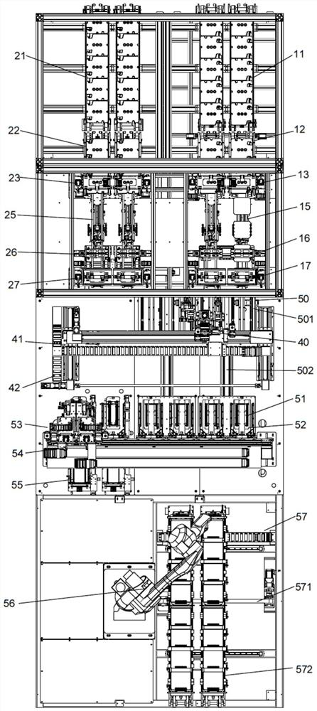
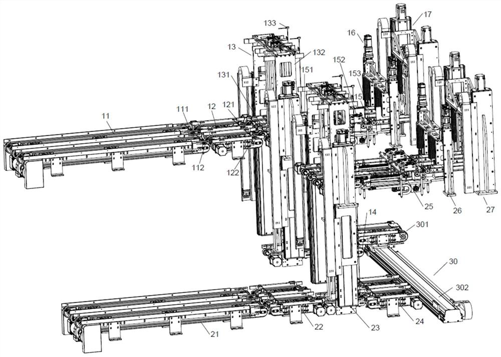
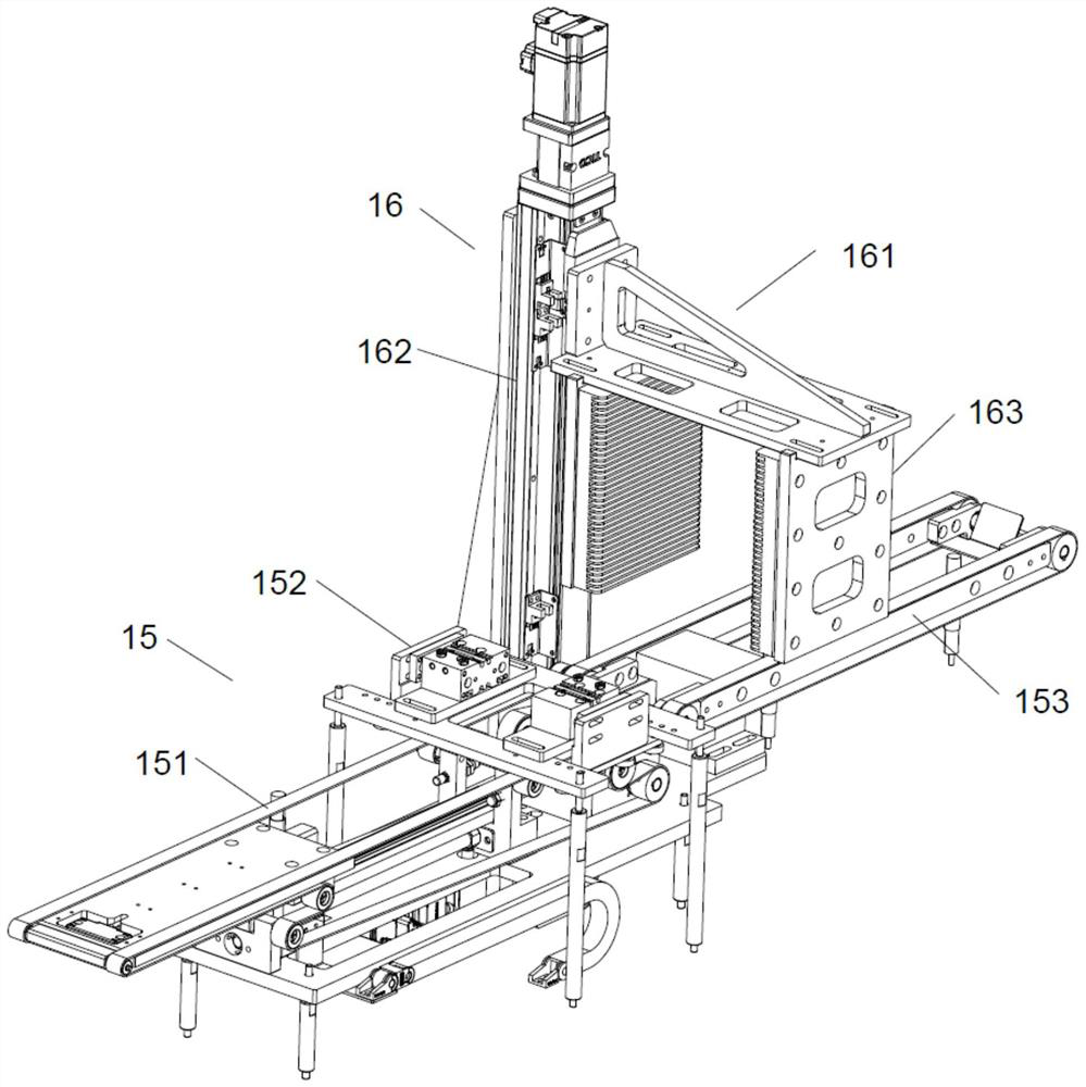
[0037] Such as Figure 1-11 As shown, a silicon wafer loading and unloading system includes a wafer guide device, a silicon wafer turning device and a handling device. The wafer guide device includes a loading guide assembly, an unloading guide assembly and a connecting loading guide assembly and the traversing conveying mechanism 30 of the unloading guide assembly, the loading guide assembly controls the silicon wafer feeding process, the unloading guide assembly controls the silicon wafer unloading process, and the traversing conveying mechanism 30 pairs the loading guide assembly and the lower The flower basket of the material guide assembly is circulated, and the silicon wafer turning device includes a silicon wafer turning mechanism 40, a silicon wafer traversing mechanism 41 and a silicon wafer offset mechanism 42, and the silicon wafer traversing mechanism 41 and the silicon wafer offset mechanism 42 controls the movement of the wafer turning mechanism 40, the silicon w...


PUM


Abstract

The invention discloses a silicon wafer feeding and discharging system which comprises a wafer guiding machine device, a silicon wafer overturning device and a carrying device, the wafer guiding machine device controls silicon wafers to flow to the silicon wafer overturning device and controls internal circulation of a basket, and the silicon wafer overturning device controls suction, overturning and separation and combination of the silicon wafers. According to the invention, a sensor is adopted to detect the full material shortage state of the flower basket, the fine control of the number of the silicon wafers is realized, a correlation sensor is adopted to detect the residual amount of the silicon wafers in the flower basket, and meanwhile, an orientation sensor is adopted to detect the orientation of the flower basket. According to the silicon wafer feeding and discharging device, the feeding process of the silicon wafers from the wafer guiding machine device to the main machine and the discharging process of the silicon wafers from the main machine to the wafer guiding machine device are achieved, and the circulating feeding and discharging process of the silicon wafers is achieved.

Description

technical field [0001] The invention belongs to the field of photovoltaics and relates to a silicon wafer loading and unloading system. Background technique [0002] In the prior art, the unloading process of the silicon wafer from the main machine to the guide machine and the feeding process from the guide machine to the main machine are operated separately, the structure is complex, the cost is high, and the two systems occupy a large space. The invention effectively solves this problem. Contents of the invention [0003] In order to overcome the deficiencies of the prior art, the present invention provides a silicon wafer loading and unloading system. [0004] In order to achieve the above object, the present invention adopts the following technical solutions: a silicon chip loading and unloading system, characterized in that it includes a chip guide device, a silicon wafer turning device and a handling device, and the chip guide device includes a loading guide assembl...

Claims


Application Information

Patent Timeline
Patent Type & Authority Applications(China)
IPC IPC(8): H01L21/677H01L31/18
CPCH01L21/67763H01L31/1804H01L31/1876Y02E10/547
Inventor 林佳继周欢时祥
Owner LAPLACE (WUXI) SEMICON TECH CO LTD
Why Eureka
Try Eureka