Backlight module and display device thereof

A backlight module and display panel technology, applied in optics, nonlinear optics, instruments, etc., can solve the problems that connectors and other electronic components cannot be placed, connectors cannot be placed, and occupy a large area, so as to improve optical efficiency And use performance, solve optical inhomogeneity, improve the effect of use performance

Pending Publication Date: 2022-03-29
CHONGQING HKC OPTOELECTRONICS TECH CO LTD +1
View PDF0 Cites 0 Cited by
  • Summary
  • Abstract
  • Description
  • Claims
  • Application Information

AI Technical Summary

Problems solved by technology

[0003] In a traditional Mini LED backlight module, besides the LED array, other electronic devices are usually placed on the circuit surface of the substrate. Since other electronic devices will absorb light in the backlight, if the area occupied by other electronic devices is too large, shadows will be formed. Seriously affect the technical performance of Mini LED, and other electronic devices occupy too much area, making it impossible to place large components such as connectors
Therefore, the traditional Mini LED backlight module has the technical problem that connectors and other electronic components cannot be placed on different surfaces of the light board

Method used


Image

  • Backlight module and display device thereof
  • Backlight module and display device thereof
  • Backlight module and display device thereof

Examples


Embodiment 1

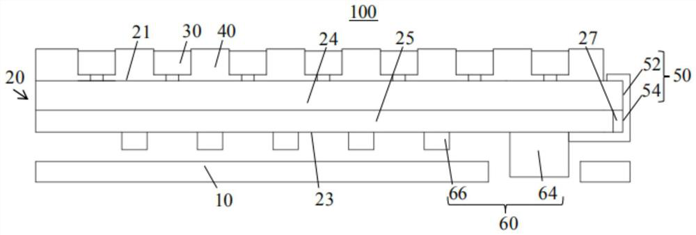
[0026] An embodiment of the present application provides a backlight module for a Mini light-emitting diode (Light-Emitting Diode, LED). see figure 1 As shown, in the backlight module 100 provided in this application, the backlight module 100 includes a backplane 10, a lamp panel 20, a plurality of light emitting elements 30, and a side wiring layer 50, wherein the lamp panel 20 includes The circuit surface 21 and the non-circuit surface 23 are opposite to each other. The backplane 10 is arranged adjacent to the non-circuit surface 23, that is, the non-circuit surface 23 faces the backplane 10, and the non-circuit surface 23 is provided with multiple An electronic device 60, a plurality of light-emitting elements 30 are arranged in an array on the circuit surface 21, and are electrically connected to the circuit surface 21, and the side wiring layer 50 extends from the circuit surface 21 to the non-circuit surface 23, and is electrically connected to multiple light-emitting e...

Embodiment 2

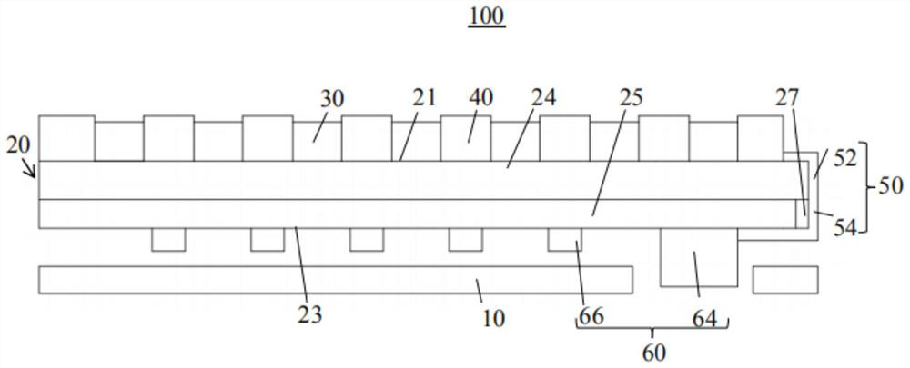
[0047] read on figure 2 , figure 2 It is a structural schematic diagram of the second embodiment of the backlight module disclosed in this application. The second embodiment of the present application and the above figure 1 The first embodiment shown is different in that: the anti-light absorption layer 40 is a reflective sheet, that is, the reflective sheet can reflect that the line surface 21 points to the light emitting element 30, and the light emitting element 30 points to the line The light from two directions on the surface 21, the anti-light absorption layer 40 is arranged on the circuit surface 21, and the anti-light absorption layer 40 is provided with a through installation hole (not marked) corresponding to the position of the light-emitting element 30. Each of the light emitting elements 30 is disposed in the mounting hole and electrically connected to the circuit surface 21 . In this embodiment, the depth of the installation hole is greater than the height o...

Embodiment 3

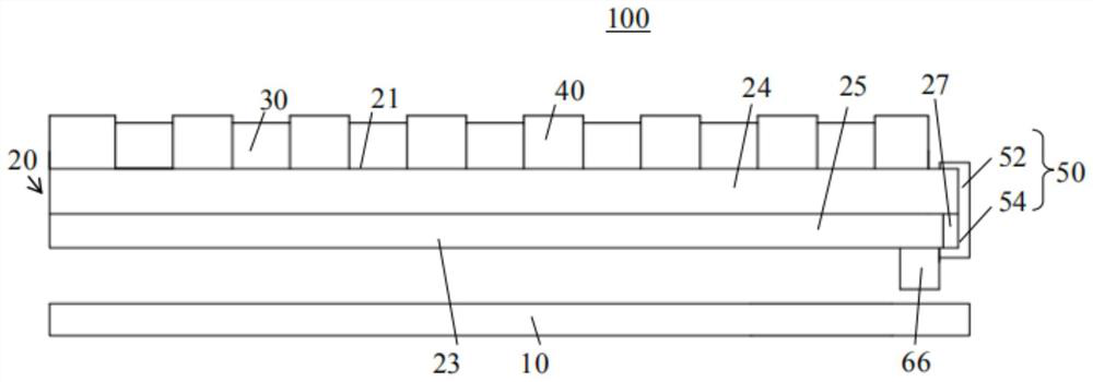
[0051] Please also refer to image 3 , image 3 It is a schematic structural diagram of the third embodiment of the backlight module disclosed in this application. The difference between the third embodiment of the present application and the first embodiment and the second embodiment above is that the electronic device 60 in the backlight module 100 only includes an electronic component 66 , ie does not include a connector 64 . The electronic component 66 is directly electrically connected to the second connection section 54, that is, the light-emitting element 30 and the electronic component 66 are directly electrically connected on the non-circuit surface 23 through the side wiring layer 50, and the electronic The element 66 provides electric energy for the normal operation of the backlight module 100 .

[0052] In one embodiment, the electronic component 66 may include but not limited to: a flexible circuit board, a carbon nanotube (Carbon Nanotube, CNT), a driver chip, ...


PUM


Abstract

The invention relates to a backlight module and a display device with the backlight module. The backlight module is used for a Mini light emitting diode. The backlight module comprises a side edge wiring layer, the lamp panel comprises a circuit surface and a non-circuit surface which are opposite in position, the back plate is arranged adjacent to the non-circuit surface, a plurality of electronic devices are arranged on the non-circuit surface, a plurality of light-emitting element arrays are arranged on the circuit surface and electrically connected with the circuit surface, and the side edge wiring layer extends from the circuit surface to the non-circuit surface. The plurality of light-emitting elements and the plurality of electronic devices are electrically connected. According to the backlight module, the light-emitting element and the electronic device are arranged on the different surfaces of the lamp panel through the side edge wiring layer, meanwhile, the situation that shadows are formed on the lamp panel due to the fact that the electronic device absorbs light is avoided, and the optical uniformity, efficiency and use performance of the backlight module are improved.

Description

technical field [0001] The present invention relates to the technical field of liquid crystal display, in particular to a backlight module for Mini light-emitting diode (Light-Emitting Diode, LED) and a display device with the backlight module. Background technique [0002] In the technical development of liquid crystal display, the backlight module is an indispensable part. Among them, the advantages of Mini LED backlight technology are very obvious. Its ability to control the backlight area and reduce the optical distance of the backlight has been improved, thereby achieving high dynamic contrast, and has the significant advantage of weakening self-illumination technology. [0003] In a traditional Mini LED backlight module, besides the LED array, other electronic devices are usually placed on the circuit surface of the substrate. Since other electronic devices absorb light in the backlight, if the area occupied by other electronic devices is too large, shadows will be for...

Claims


Application Information

Patent Timeline
Patent Type & Authority Applications(China)
IPC IPC(8): G02F1/13357G02F1/1337
CPCG02F1/133603G02F1/133612G02F1/133605G02F1/133606G02F1/133723
Inventor 胡晓刚李荣荣
Owner CHONGQING HKC OPTOELECTRONICS TECH CO LTD
Why Eureka
Try Eureka