Supercharge Your Innovation With Domain-Expert AI Agents!

Method for manufacturing ceramic electronic component

A technology of electronic components and manufacturing methods, which is applied in the parts, electrical components, circuits and other directions of fixed capacitors, can solve the problems of hindering the compactness of the electrode layer from burning, and achieve the effect of strong bearing capacity and not easy to be damaged.

Pending Publication Date: 2022-03-29
MURATA MFG CO LTD
View PDF12 Cites 0 Cited by
  • Summary
  • Abstract
  • Description
  • Claims
  • Application Information

AI Technical Summary

Problems solved by technology

However, if the technology described in Patent Document 1 is used to make the fired electrode layer have voids and at the same time reduce the thickness of the fired electrode layer, the presence of voids will hinder the compactness of the fired electrode layer.

Method used


Image

  • Method for manufacturing ceramic electronic component
  • Method for manufacturing ceramic electronic component
  • Method for manufacturing ceramic electronic component

Examples


Embodiment Construction

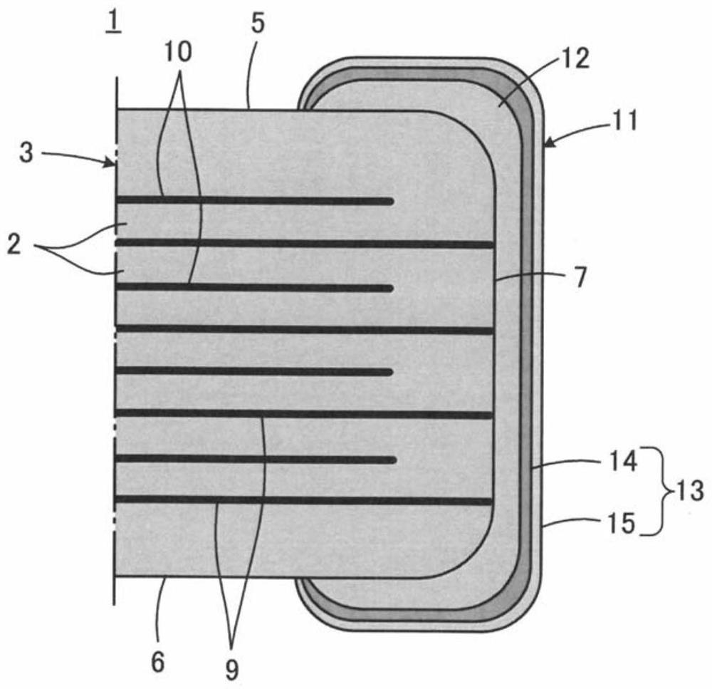
[0037] When describing a ceramic electronic component produced by applying the production method according to the present invention, a laminated ceramic capacitor is used as an example of a ceramic electronic component.

[0038] refer to figure 1 A multilayer ceramic capacitor 1 includes a ceramic body 3 including a plurality of stacked ceramic layers 2 , and the plurality of ceramic layers 2 include dielectric ceramics. The ceramic body 3 has a first main surface 5 and a second main surface 6 facing each other, a first end surface 7 connecting the first main surface 5 and the second main surface 6, and a first end surface 7 connected to the first main surface 5 and the second main surface 6, although not shown. The second end face facing the first end face 7, although not shown, also has a figure 1 1st side surface and 2nd side surface which extend parallel to paper surface and oppose mutually.

[0039] The ceramic body 3 further includes a plurality of first internal elect...


PUM

PropertyMeasurementUnit
thicknessaaaaaaaaaa
particle sizeaaaaaaaaaa
Mohs hardnessaaaaaaaaaa

Abstract

Provided is a method for manufacturing a ceramic electronic component provided with an external electrode capable of relieving mechanical stress and thermal stress from the outside in a mounted state of the ceramic electronic component. The step of providing the external electrode includes: a step of forming a fired electrode layer by applying a conductive paste containing a conductive metal and glass so as to cover a portion of the ceramic body where the internal electrode is exposed and firing the same; and a step for forming a plating film on the surface of the fired electrode layer by a plating method. The burning electrode layer includes a metal portion and a glass portion distributed in a state of being in contact with the metal portion. After the sintered electrode layer is formed, the surface of the sintered electrode layer is subjected to drum treatment or sand blasting treatment using a powder having a Mohs hardness equal to or less than the Mohs hardness of the ceramic body, and cracks capable of alleviating external mechanical stress and thermal stress are formed in the glass portion of the sintered electrode layer.

Description

technical field [0001] The present invention relates to a method of manufacturing a ceramic electronic component, and more particularly to a method of forming an external electrode on the surface of a ceramic body included in the ceramic electronic component. Background technique [0002] Chip-shaped ceramic electronic components such as multilayer ceramic capacitors include: a ceramic body having internal electrodes partially exposed on the surface; and external electrodes provided on a part of the surface of the ceramic body and electrically connected to the internal electrodes. The external electrodes generally include: a baked electrode layer including, for example, a conductive metal such as copper and glass; and a plating film provided on the surface of the baked electrode layer. The plated film is formed by electroplating, and includes, for example, a nickel layer and a tin layer on the nickel layer. [0003] The ceramic electronic component as described above is mou...

Claims


Application Information

Patent Timeline
Patent Type & Authority Applications(China)
IPC IPC(8): H01G4/30H01G4/005H01G4/008
CPCH01G4/306H01G4/005H01G4/008H01G4/12H01G4/30H01G4/2325H01G4/232
Inventor 喜住哲也横田雄介
Owner MURATA MFG CO LTD
Features
  • R&D
  • Intellectual Property
  • Life Sciences
  • Materials
  • Tech Scout
  • Unparalleled Data Quality
  • Higher Quality Content
  • 60% Fewer Hallucinations
Learn More