Optical module

An optical module and MOS tube technology, applied in the field of optical communication, can solve the problems of pulling down the I2C signal line, pulling down the I2C signal, affecting the normal communication of other module products, etc., so as to ensure normal communication and avoid the level being pulled down. Effect

Pending Publication Date: 2022-04-05
HISENSE BROADBAND MULTIMEDIA TECH
0 Cites 0 Cited by

AI-Extracted Technical Summary

Problems solved by technology

[0003] During the power-on process of the optical module, the MCU working state of the optical module is uncontrollable, and an uncontrollable signal is generated, and the level of the I2C signal line is temporarily pulled down by the uncontrollable signal, such as Image 6 The levels of the SDA signal line and the SCL ...

Method used

Adopt the assembly mode that upper casing 201, lower casing 202 combine, be convenient to circuit board 105, devices such as optical transceiver devices are installed in the casing, can form these devices by upper casing 201, lower casing 202 Encapsulation protection. In addition, when assembling components such as the circuit board 105 , it is convenient to deploy positioning components, heat dissipation components and electromagnetic shielding components of these components, which is conducive to automatic implementation of production.
Fig. 13 is a schematic diagram of the I2C signal level change in the power-on process of the optical module after the circuit optimization design according to some embodiments; Fig. 14 is a schematic diagram of the I2C signal quality in the power-on process of the optical module after the circuit optimization design according to some embodiments ; It can be seen from Figure 13 and Figure 14 that after optimizing the I2C circuit, the levels of the SDA signal and the SCL signal remain stable during the hot-swapping process of the optical module, and there is no short-term pull-down situation; and the I2C is in the There is no abnormality in the signal during the communication process, and the signal remains stable.
In actual application, optical module and upper computer carry out communication and finish, and optical module sends response signal after receiving signal, because there is difference in the driving ability of optical module and upper computer, promptly driving ability does not match, causes SDA signal Or negative overshoot or positive overshoot of the SCL signal, showing glitches in the SDA signal or SCL signal, which will affect the service life of the optical module and the host computer in the long run. For this reason, in the embodiment of the present application, a filter circuit is also added, and the specific implementation is as follows: a first filter circuit is connected in parallel at the SDA slow-start circuit, and the first filter circuit includes a first filter capacitor; a second filter circuit is connected in parallel at the SCL slow-start circuit , the second filter circuit includes a second filter capacitor; the first filter capacitor and the second filter capacitor can absorb signal quality cracking caused by mismatching driving capabilities, thereby avoiding glitches in the SDA signal or SCL signal and optimizing signal quality.
In the embodiment of the application, SDA slow-starting circuit and SCL slow-starting circuit respectively delay conduction SDA signal line and SCL signal line after receiving the power supply slow-starting circuit signal, by SDA slow-starting circuit and SCL slow-starting circuit control The conduction time of the SDA signal line and the SCL signal, and then delay the conduction of the corresponding SDA signal line and SCL signal line, and realize the delay conduction of the I2C signal line, so as to avoid the level of the I2C signal being pulled down during the power-on process of the optical module , thus ensuring normal communication.
In the embodiment of the present application, by optimizing the circuit design of I2C, the timing sequence of I2C signal line conduction and power supply conduction is adjusted, and the I2C is turned on after the MCU is started, so as to avo...

Abstract

The optical module comprises a circuit board, an MCU and a golden finger, the surface of the circuit board is provided with an SDA signal line and an SCL signal line, a power supply slow start circuit is arranged between the golden finger and an MUC power supply pin, an SDA slow start circuit is arranged between the golden finger and an SDA interface, and an SCL slow start circuit is arranged between the golden finger and an SCL interface. The power supply slow start circuit is electrically connected with the SDA slow start circuit and the SCL slow start circuit. The SDA slow start circuit and the SCL slow start circuit respectively conduct the SDA signal line and the SCL signal line in a delayed mode after receiving a power supply slow start circuit signal, the conduction time of the SDA signal line and the SCL signal line is controlled through the SDA slow start circuit and the SCL slow start circuit, then the corresponding SDA signal line and the SCL signal line are conducted in a delayed mode, the I2C signal line is conducted in a delayed mode, and therefore the I2C signal line is switched on in a delayed mode. And the level of the I2C signal is prevented from being lowered in the power-on process of the optical module, so that normal communication is ensured.

Application Domain

Electrical connection printed elementsElectromagnetic transceivers +1

Technology Topic

PhysicsHemt circuits +3

Image

  • Optical module
  • Optical module
  • Optical module

Examples

  • Experimental program(1)

Example Embodiment

[0028] The technical solutions in some embodiments in the present disclosure will be described below in conjunction with the accompanying drawings. Based on the embodiments provided by the present disclosure, all other embodiments obtained by those of ordinary skill in the art are the scope of the present disclosure.
[0029] Unless otherwise requested elsewhere, the term "comprised" and other forms, including COMPRISES, "and" comprises "and current forms, including (COMPRISES),", "," Explain that it is open, meaning, ie "contain, but not limited to". In the description of the specification, the term "one embodiment", "some embodiment (some embodiment (some embodiment," ExemPlary Embodiments, "Example," Specific "," Specific Example) "or" Some Examples ", etc., is intended to indicate specific features, structures, materials, or characteristics associated with this embodiment or examples, include at least one embodiment or example in the present disclosure. The schematic representation of the above terms does not necessarily refer to the same embodiment or example. Moreover, the specific features, structures, materials, or features may be included in any one or more embodiments or examples in any suitable manner.
[0030] Hereinafter, the term "first", "second" is used only for the purpose of describing, and cannot be understood as an indication or implies a relative importance or implicitly indicated the number of techniques indicated. Thus, features with "first", "second" may be indicated or implicitly including one or more of this feature. In the description of the embodiments of the present disclosure, the meaning of "multiple" is two or more unless otherwise stated.
[0031] When describing some embodiments, "coupling" and "connection" may be used and expressed. For example, a "connection" may be used when describing some embodiments to indicate that two or more of the above components are directly physically in contact with each other. As another example, the term "coupled" may be used when describing some embodiments to indicate that two or more components are directly physically in contact or electrical contact. However, the term "coupling" or "communication" may also mean that two or more components are not directly in contact with each other, but still cooperate or interact with each other. The embodiments disclosed herein are not necessarily limited to the contents of this article.
[0032] "At least one of A, B, and C" has the same meaning as "at least one of" A, B or C ", including combinations of the following A, B, and C: only A, only b, only C, A and B Combination, combination of A and C, combination of B and C, and combinations of A, B and C.
[0033] "A and / or B", including the following three combinations: only A, only B, and A and B combination.
[0034] The use of "suitable for" or "configured" herein means that open and inclusive languages ​​do not exclude devices suitable for or configured to perform additional tasks or steps.
[0035] As used herein, "about", "approximate" or "approximate" includes the values ​​of the illustrated values ​​and an average value in the acceptable deviation range of specific values, wherein the acceptable deviation range is, such as one of ordinary skill in the art. Considering the measurements being discussed and the error associated with a particular amount of measure (ie, the limitations of the measurement system) are determined.
[0036] In optical communication technology, the information to be transmitted is carried out, and the optical signal carrying information is transmitted to information processing devices such as information transmission devices such as optical fibers or optical waveguides to complete information transmission. Since the optical signal has passive transmission characteristics when transmitting in a fiber or optical waveguide, low cost, low loss information transmission can be achieved. Further, the signal transmitted by the information transmission apparatus such as the fiber or optical waveguide is an optical signal, and the information processing apparatus such as the computer can identify and process is an electrical signal, so in order to perform information processing equipment such as an optical fiber or optical waveguide and a computer. An information connection is required, and the mutual conversion of electrical signals and optical signals is required.
[0037] The optical module realizes the mutual conversion function of the optical signal and the electrical signal in the field of optical fiber communication technology. The optical module includes a light port and an electrical port, and the optical module realizes optical communication with the information transmission device such as the optical fiber or optical waveguide through the optical port. The electrical connection between the optical network terminal (eg, a light cat) is realized by the electrical port. Mainly used to achieve power supply, I2C signal transmission, data signal transmission, and grounding, etc.; the optical network terminal transmits electrical signals to computer and other information processing devices via network line or wireless fidel technology (Wi-Fi).
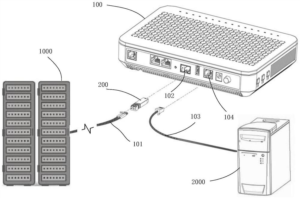
[0038] figure 1 A connection relationship diagram of an optical communication system according to some embodiments. Such as figure 1 As shown, the optical communication system mainly includes a remote server 1000, a local information processing apparatus 2000, an optical network terminal 100, an optical module 200, an optical fiber 101, and a network cable 103;
[0039]One end of the optical fiber 101 is connected to the remote server 1000, and the other end is connected to the optical network terminal 100 through the optical module 200. The fiber optic itself can support a remote signal transmission, such as signal transmission of thousands of meters (6 km to 8 km), based on this, if the repeater is used, the ultra-long distance transmission can be realized. Thus in a usual optical communication system, the distance between the distal server 1000 and the optical network terminal 100 can usually reach thousands of meters, hundreds of kilometers or hundreds of kilometers.
[0040] One end of the network cable 103 is connected to the local information processing device 2000, and the other end is connected to the light network terminal 100. Local information processing device 2000 can be any of the following devices: routers, switches, computers, mobile phones, tablets, televisions, etc.
[0041] The physical distance between the distal server 1000 and the optical network terminal 100 is larger than the physical distance between the local information processing device 2000 and the optical network terminal 100. The connection between the local information processing device 2000 and the remote server 1000 is done by the optical fiber 101 and the network cable 103; and the connection between the optical fiber 101 and the network cable 103 is done by the optical module 200 and the optical network terminal 100.
[0042] The optical module 200 includes a light port and an electrical port. The optical port is configured to be connected to the optical fiber 101 such that the optical module 200 is configured to establish a two-way optical signal connection; the electromost is configured to access the optical network terminal 100, so that the optical module 200 is established two-way network terminal 100. Electrical signal connection. The optical module 200 achieves mutual conversion of the optical signal and the electrical signal such that the optical fiber 101 is connected to the optical network terminal 100. Example, the optical signal from the optical fiber 101 is converted from the optical module 200 into an electrical signal into the optical network terminal 100, and the electrical signal from the optical network terminal 100 is converted by the optical module 200 into the optical signal input to the optical fiber 101.
[0043] The optical network terminal 100 includes a housing (housing) that is substantially long, and an optical module interface 102 and a network cable interface 104 disposed on the housing. The optical module interface 102 is configured to access the optical module 200 such that the optical network terminal 100 is configured to establish a two-way electrical signal connection; the network cable interface 104 is configured to access the network cable 103 such that the optical network terminal 100 and the network cable 103 Establish a two-way electrical signal connection. The optical module 200 is connected to the network cable 103 through the optical network terminal 100. In the example, the optical network terminal 100 transmits the electrical signal from the optical module 200 to the network cable 103, and the signal from the network cable 103 is transmitted to the optical module 200, so the optical network terminal 100 can monitor the optical module 200 as the host machine of the optical module 200. work. Optical Module 200 may include Opticalline Terminal (OLT), etc.
[0044] The distal server 1000 creates a two-way signal transmission channel between the local information processing device 2000 by the optical fiber 101, the optical module 200, the optical network terminal 100, and the network cable 103.
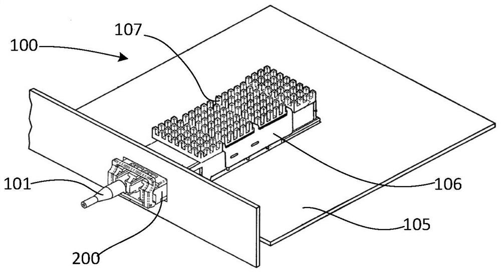
[0045] figure 2 In order to clearly display the connection relationship between the optical module 200 and the optical network terminal 100 in order to clearly display the connection between the optical module 200 and the optical network terminal 100. figure 2 Only the structure related to the optical module 200 is shown in the optical network terminal 100. Such as figure 2 As shown, the optical network terminal 100 also includes a PCB circuit board 105 disposed within the housing, a cage 106 disposed on the surface of the PCB circuit board 105, and an electrical connector disposed inside the cage 106. The electrical connector is configured to access the electrical port of the optical module 200; the heat sink 107 has a bumpy portion such as a fins such as a heat dissipation area.
[0046] In the cage 106 of the optical network terminal 100, the optical module 200 is fixed by the cage 106, and the heat generated by the optical module 200 is conducted to the cage 106, and then diffused by the heat sink 107. After the optical module 200 is inserted into the cage 106, the electrical port of the optical module 200 is connected to the electrical connector inside the cage 106, so that the optical module 200 is connected to the optical network terminal 100 to establish a two-way electrical signal connection. Further, the optical port of the optical module 200 is connected to the optical fiber 101, so that the optical module 200 is connected to the optical fiber 101 to establish a two-way electrical signal connection.
[0047] image 3 For a structural diagram of a light module according to some embodiments, Figure 4 An exploded view of a light module according to some embodiments. Such as image 3 and Figure 4 As shown, the optical module 200 includes a housing, a circuit board 105 and a light transceiver device disposed in the housing;
[0048] The housing includes an upper casing 201 and a lower housing 202, and the upper casing 201 is ligated to the lower casing 202 to form the housing having two openings 204 and 205; the outer contour of the housing generally presents a square body.
[0049] In some embodiments of the present disclosure, the lower housing 202 includes a bottom plate and two lower side plates located on both sides of the bottom plate, and the upper casing 201 including a cover, and a cover side and a cover vertical setting. The two upper plates are bonded from two sidewalls to two side panels to achieve the upper housing 201 lies on the lower casing 202.
[0050] The direction in which the two openings 204 and 205 is located may be coincident with the length direction of the optical module 200 or may be inconsistent with the length direction of the optical module 200. Example, the opening 204 is located at the end of the optical module 200 ( image 3 The left end), the opening 205 is also located at the end of the optical module 200 ( image 3 Right end). Alternatively, the opening 204 is located at the end of the optical module 200, and the opening 205 is located on the side of the optical module 200. Among them, the opening 204 is the electrical port, the gold finger of the circuit board 105 projects from the opening 204, inserted into the upper machine (such as the optical network terminal 100); the opening 205 is a light port, configured to access the outer fiber 101 to make the optical fiber 101 Connect the optical transceiver inside the optical module 200.
[0051] Using the upper housing 201, the lower case 202 is combined with the assembly method to facilitate mounting the circuit board 105, the optical transceiver, etc., by the upper housing 201, and the lower housing 202 can form package protection for these devices. Further, in the assembly circuit board 105 and other devices, it is convenient for the positioning components, heat dissipation members, and the deployment of the electromagnetic shielding components, which are conducive to the production of automation.
[0052] In some embodiments, the upper housing 201 and the lower case 202 generally be made of a metal material, facilitating electromagnetic shielding and heat dissipation.
[0053] In some embodiments, the optical module 200 further includes a unlocking member 203 located in the outer wall of its housing, and the unlocking member 203 is configured to implement a fixed connection between the optical module 200 and the host computer, or unlike the optical module 200 and the host computer. Fixed connection.
[0054] Example, the unlocking member 203 is located at the outer wall of the two lower plates of the lower case 202, including a engaging member that matches the cage of the host computer (eg, the cage 106 of the optical network terminal 100). When the optical module 200 is inserted into the cage of the host computer, the engaging member of the unlocking member 203 fixes the optical module 200 in the cage of the host computer; when the unlocking member 203 is pulled, the engagement member of the unlocking member 203 is moved, and then changes. The connection between the part is engaged with the host computer to release the engagement relationship between the optical module 200 and the host computer, so that the optical module 200 can be extracted from the cage of the host computer.
[0055] The circuit board 105 includes a circuit trace, an electronic component, and a chip that connects the electronic components and the chip to the circuit design through the circuit trace to achieve power supply, electrical signal transmission, and grounding. Electronic components may, for example, include a capacitor, a resistor, a transistor, a metal-oxide-semiconductor field effector (MOSFET). Chips can include, for example, microController Unit, MCU, Limiting Amplifier, Clock Data Recovery, CDR, Power Management Chip, Digital Signal Processing, DSP chip .
[0056] The circuit board 105 is generally a hard circuit board, and the hard circuit board can also carry the carrying effect due to its relatively hard material, such as the hard circuit board to carry the chip; the hard circuit board can also be inserted into the electrical connector in the upper machine cage. .
[0057] The circuit board 105 also includes a gold finger formed on the surface of its end, and the gold finger consists of multiple pins independently of each other. The circuit board 105 is inserted into the cage 106, and is connected by a gold finger to the electrical connector within the cage 106. The gold finger can be provided only on the surface of the circuit board 105 (eg, Figure 4 The upper surface shown) may also be disposed on the surface on both sides of the circuit board 105 to accommodate the number of pins. The gold finger is configured to establish an electrical connection with the host computer to achieve power supply, grounding, I2C signal transmission, data signal transmission, and the like. Of course, a flexible circuit board is also used in some optical modules. Flexible circuit boards are generally used in conjunction with hard circuit boards as a hard circuit board.
[0058] The optical transceiver includes a light transmitting secondary module and a light receiving secondary module. The light transmitting module 206 and the light receiving secondary module 207 are respectively used to realize the transmission of the optical signal and the reception of the optical signal. The optical transmitting module 206 and the light receiving secondary module 207 may also bond together to form a light-proof one. Among them, the light emission module 206 includes an optical emission chip and a backlight detector, and the light receiving secondary module 207 includes a light receiving chip.
[0059] The light transmitting module 206 and the light receiving secondary module 207 are respectively used to realize the transmission of the optical signal and the reception of the optical signal. In this embodiment, the optical emission module 206 can be encapsulated by the coaxial TO, physically separated from the circuit board, and is electrically connected by a flexible plate; the light receiving secondary module 207 also adopts the coaxial TO package, physically separated from the circuit board, by flexibility The board is electrically connected. In another common implementation, the surface of the circuit board 105 can be provided; additionally, the optical transmitting secondary module 206 and the light receiving secondary module 207 may be combined together to form a light-proof one.
[0060] The optical module and the host computer can be transmitted via the I2C bus, and the I2C signal line includes an SDA signal line and a SCL signal line, wherein the SDA line is a data line, the SCL line is a clock line.
[0061] The interface of the I2C bus is directly in the assembly, the space occupies a relatively small space, less space, and reduces the number of pins of the chip; the I2C bus realizes data transmission mounted between the fully devices.
[0062] When the SDA signal line of the I2C bus and the SCL signal line are at high levels, the bus is in an idle state, that is, the bus is released, the SDA signal line and the SCL signal line are connected to the power source through the pull-up resistor. The change in the high and low level of the signal line only allows the SDA to remain stable when the SCL signal line is at a low level, when the SCL signal line is in a high level, and the information on the SDA is active.
[0063] In the present application embodiment, the optical module supports the hot-swap function, and the power supply of the optical module power supply is reduced by the design of the optical module power supply, which can effectively solve the surge in the hot-swing of the optical module. The current is damaged by the module. The optical module power is slow and the circuit structure is Figure 5As shown, the optical module power reducing circuit includes parallel third resistance R3 and the third capacitor C3, and then in series with the third MOS tube, forming a power reducing circuit; MOS tube includes gate G, source S and drain D D The MOS tube is used as the switching element. The working state includes a state and an on state; the MOS tube is used as a voltage control element, which is mainly determined by the voltage between the gate G and the source S, which is greater than the on-threshold voltage. When the surface of the p-type silicon under the gate g has a strong reverse shape, forming an N-type channel of the connection source region and the drain region, generating a drain current, a MOS tube conduction; in turn, when the voltage is less than the on-threshold voltage, The MOS tube is not turned on. In the optical module power supply, the third resistor R3 is a current limiting resistor. The third capacitor C3 is the energy storage capacitor, and the third resistor R3 is charged to the third capacitor C3, and the voltage applied to the MOS tube is controlled by controlling the charging time. However, by controlling the charging time, the voltage control MOS tube can be realized, and then the operation of the MOS tube is controlled, and the activation of the optical module power supply is controlled, so the time to charge the third resistor R3 to the third capacitor C3, light can be realized. The slowdown of the module power supply, avoiding the surge current generated by the optical module during hot-swapping, the surge voltage generated against the module is damaged.
[0064] During the optical module power-on, the optical module power is slowed down under the action of the optical module power supply, and the power supply time is later than the I2C signal on time. At this point, the MCU of the optical module has not been activated, the working state is uncontrollable, An uncontrollable signal is generated, and the level on the I2C signal line is shorter, which can be seen that during this process, the timing relationship between the MCU start and the I2C signal is: first I2C signal is turned on, then MCU starts; Image 6 The level of the SDA signal line SCL signal line is lowered, thereby affecting normal communication of other optical modules mounted on the I2C signal line. As can be seen from the above, the I2C signal will be pulled, affecting normal communication of other module products during the optical module. Image 6 The signal line on the middle position is the SDA signal line, and the signal line in the position is the SCL signal line, from Image 6 As can be seen, the level of the SDA signal line and the SCL signal line is low in an instantaneous moment. Specific abnormal reference Figure 7 , Figure 7 The I2C signal quality abnormality is schematically illustrated in the optical module on the optical module according to some embodiments.
[0065] In order to solve the above problems, the design idea of ​​the present application example is: SDA-repellent circuit and SCL reducing circuit are respectively provided on the SDA signal line and the SCL signal line; the SDA reducing circuit and SCL reducing circuit are received. After the circuit signal is delayed, the SDA signal line and the SCL signal line are turned on, and the SDA signal line and the SCL return circuit are controlled by the SDA signal line and the SCL signal line, which in turn turns on the corresponding SDA signal line. And the SCL signal line, realize the latency on the I2C signal line, avoiding the I2C signal during the optical module on the power module, and then guaranteed normal communication.
[0066] The scheme of the present application embodiments will be specifically described with reference to the accompanying drawings.
[0067] Such as Figure 8 The relationship between the power-down circuit, the SDA mobilization circuit, the SDA mobilization circuit; the upper machine and the optical module implement a communication connection through the gold finger, the MCU is equipped with a power supply pin, an SDA interface, and an SCL interface, in a gold finger and MUC. The power supply pin is equipped with a power-slow circuit, and there is an SDA-slow circuit between the gold finger and the SDA interface. It is equipped between the gold finger and the SCL interface, and the power-down circuit is slow and SDA. Status The circuit and SCL slow circuit are electrically connected.
[0068] The SDA Rocking Circuit and SCL Slow Circuit delay the SDA signal line and the SCL signal line after receiving the power supply mobilization, and control the SDA signal line and the SCL signal line via the SDA reducing circuit and the SCL. Tight time, in turn, turn on the corresponding SDA signal line and the SCL signal line.
[0069] It will be appreciated that the start timing of the MCU and the start timing of the I2C signal line can be adjusted according to actual needs. If the SDA signal line and the SCL signal line are started after the MCU is activated, even before the MCU starts the I2C signal line, SDA slow The starting circuit and SCL mwing circuit can also be implemented: the SDA signal line and the SCL signal line are turned on after receiving the power moke circuit signal, respectively.
[0070] Such as Figure 9 As shown, the upper machine has an SDA interface and an SCL interface. The MCU of the optical module also has an SDA interface and an SCL interface. The SDA pin and SCL pin are provided on one end of the optical module board, and the SDA interface of the optical module is passed. The SDA pin of the gold finger is electrically connected to the SDA interface of the host computer to form an SDA total signal line; the SCL interface of the optical module is electrically connected to the SCL pin of the gold finger to electrically connect, form the SCL total signal line.
[0071] The structure of the SDA total signal line on the optical module board includes: one end is the SDA pin of the gold finger, one end is the SDA interface of the MCU, that is, the SDA pin of the gold finger and the SDA interface of the MCU forms an optical module SDA signal line. , Accordingly, the SCL pin of the gold finger and the SCL interface of the MCU form the SCL signal line of the optical module.
[0072] Such as Figure 10 As shown, the SDA-proof circuit is set on the SDA signal line of the optical module, and the SCL-slow circuit is set on the SCL signal line of the optical module, and the SDA rests the circuit can delay the SDA signal line, and it is realized in the MUC startup. Tong SDA signal line; the SCL reducing circuit can delay the SCL signal line, realize the SCL signal line after the MCU is started; in turn turn on the I2C bus, and the I2C bus is turned on after the MCU startup.
[0073] Figure 11 and Figure 12 Structure schematic of SDA plug circuit and SCL reducing circuit is shown separately.
[0074] Such as Figure 12 As shown, the SCL reducing circuit includes a first MOS tube, a first ventilation control assembly, and a first MOS tube to be connected in series with the first turning control assembly, and the first turning control component is used to control the first An MOS tube is turned on and disconnected.
[0075] The drain D of the first MOS tube is electrically connected to the SDA pin of the gold finger. The source S of the first MOS tube is electrically connected to the SDA interface of the MCU. The gate G and the first all-wheel-off control assembly of the first MOS tube are electrically connected. connect.
[0076] In the present application embodiment, the first ventilation control assembly includes a first resistance and a first capacitor in parallel, by controlling the first resistance as a first capacitance power supply time to change the voltage of the gate G of the first MOS tube.
[0077] It should be noted that the first all-wheel control assembly in the present application embodiment may be other forms of component structures, not limited to the first resistance and the first capacitance of each other.
[0078] The MOS tube is used as a voltage control element, which is mainly determined by the voltage between the gate G and the source S, when the voltage is larger than the on-threshold voltage, the surface of the p-type silicon surface under the gate G occurs strongly, formed The N-type channel of the pass source region and the drain area produces a drain current, the MOS tube is turned on; in turn, the MOS tube is not turned on when the voltage is less than the on-threshold voltage. In the SDA reset circuit, the first resistor R1 is a current limiting resistor, and the first capacitor C1 is a capacitor, and the first resistor R1 is charged to the first capacitor C1, and the voltage applied to the first MOS tube is controlled by controlling the charging time. That is, the voltage to control the first MOS tube can be realized by controlling the charging time, and then controls the on time of the MOS tube, thereby controlling the on-time on the optical module SDA signal line.
[0079] In the present application embodiment, by recording the MCU startup time, it is possible to determine the time to charge the first capacitor C1 to the first capacitor C1, and then determine the voltage applied to the first MOS tube, further determine the on-time on the SDA signal line, guarantee The on time of the SDA signal line is later than the MCU startup time, so the first resistor R1 is determined by the MCU startup time to the first capacitor C1.
[0080] In the present application embodiment, the first MOS pipe conduction time is controlled by controlling the voltage applied to the first MOS tube, thereby controlling the on-time of the SDA signal line, and then start the SDA signal line after the MCU is activated.
[0081] Such as Figure 11 As shown, the SCL reducing circuit includes a second MOS tube, a second all-wheel-off control assembly, and the second MOS tube is connected in series with the second turmoil control assembly, and the second interruption control component is for Control the conduction and disconnection of the second MOS tube.
[0082] The drain D of the second MOS tube is electrically connected to the SCL pin of the golden finger. The source S of the MOS tube is electrically connected to the SCL interface of the MCU, and the gate G of the second MOS tube and the first Secondary to control the component electrical connection.
[0083] In the present application embodiment, the second ventilation control assembly includes a second resistor R2 and a first capacitor C2 in parallel, by controlling the second resistor R2 as the first capacitor C2 to change the gate G of the second MOS tube. Voltage.
[0084] It should be noted that the second turmoil control assembly in the present application embodiment may be other forms of component structures, not limited to the second resistance and the second capacitance of each other.
[0085] The MOS tube is used as a voltage control element, which is mainly determined by the voltage between the gate G and the source S, when the voltage is larger than the on-threshold voltage, the surface of the p-type silicon surface under the gate G occurs strongly, formed The N-type channel of the pass source region and the drain area produces a drain current, the MOS tube is turned on; in turn, the MOS tube is not turned on when the voltage is less than the on-threshold voltage. In the SCL regeneration circuit, the second resistor R2 is a current limiting resistor. The second capacitor C2 is a capacitor, and the second resistor R2 is charged to the second capacitor C2, and the voltage applied to the second MOS tube is controlled by controlling the charging time. That is, the voltage to control the second MOS tube can be realized by controlling the charging time, thereby controlling the on time of the MOS tube, thereby controlling the on-time on the optical module SCL signal line.
[0086] In the present application embodiment, by recording the MCU startup time, it is possible to determine the time of charging the second resistor R2 to the second capacitor C2, and then determine the voltage applied to the second MOS tube, further determine the on-time on the SCL signal line, guarantee The on-time of the SCL signal line is later than the MCU startup time, and therefore, the second resistor R2 is determined by the MCU startup time by the MCU startup time to the second capacitor C2.
[0087] In the present application embodiment, the second MOS pipe conduction time is controlled by controlling the voltage applied to the second MOS tube, thereby controlling the on-time of the SCL signal line, and then start the SCL signal line after the MCU is started.
[0088] Therefore, the SDA regeneration circuit is provided on the SDA signal line of the optical module, and the SCL reducing circuit is set on the SCL signal line of the optical module, and the voltage applied to the corresponding MOS tube is controlled by control, and the MOS pipe is controlled. Controlling the on-time of the SDA signal line, realizing the latency on the SDA signal line, further implementation of the SDA signal line after the MUC is started; the SCL reducing circuit can delay the SCL signal line, specifically by control application in the corresponding MOS The voltage on the tube, controls the MOS pipe conduction time, and then controls the on-time on the SCL signal line, and realizes the delay-on-SCL signal line, further implementation of the SCL signal line after the MUC is started; in turn turn on the I2C bus Realization After the MCU is started, the I2C bus party is turned on.
[0089]In the present application embodiment, the on-time of the SDA signal line and the SCL signal is controlled by the SDA reducing circuit and the SCL reducing circuit, and thereby turning through the SDA-reducing circuit and SCL reducing circuit delay on the corresponding SDA signal line and SCL. The signal line, realizes the delay-on I2C signal line, ensuring that the I2C signal line is maintained after the MCU is activated, and the I2C signal is avoided in the optical module, and thereby ensuring normal communication.
[0090] In the present application embodiment, by optimizing the circuit design of the I2C, the I2C signal line is adjusted and the power supply turning time is adjusted. After the MCU is activated, then the I2C is turned on, and the I2C signal is avoided, and it is lowered during the power generation process to ensure normal communication.
[0091] Figure 13 A variation of the I2C signal level during the power module is optimized for the circuit optimization of the circuit in accordance with some embodiments; Figure 14 In order to optimize the design of the I2C signal quality during power generation process according to some embodiments; Figure 13 and Figure 14 It can be seen that by optimizing the I2C circuit, the level of the SDA signal and the SCL signal remains stable during the hot-insertion of the optical module, and does not appear short-temporarily; and the I2C is not present during communication. Abnormal, the signal remains stable.
[0092] In practical applications, the optical module communicates with the upper machine, and the optical module issues a response signal after receiving the signal, since there is a difference in the driving capability of the optical module and the host computer, that is, the driving capability does not match, resulting in SDA signal or SCL signal. There is a negative hybrid or positive hush, showing a burr in the SDA signal or SCL signal, which will affect the life of the optical module and the host computer. To this end, the filter circuit is also increased in the present application, and the first filter circuit includes a first filter capacitor at the SDA reducing circuit, and the first filter circuit includes a first filter capacitor; a parallel second filter circuit at the SCL The second filter circuit includes a second filter capacitor; the first filter capacitor and the second filter capacitor can absorb the signal quality cracking due to the mismatch of the driving capacity, thereby avoiding the inclusion in the SDA signal or SCL signal, optimizing the signal quality.
[0093] In the present application embodiment, the SDA retardation circuit and the SCL reducing circuit delay the SDA signal line and the SCL signal line after receiving the power source molten circuit signal, and the SDA signal line is controlled by the SDA-proof circuit and the SCL. The on-time of the SCL signal, in turn, turn on the corresponding SDA signal line and the SCL signal line, realize the delay on the I2C signal line, avoiding the I2C signal during the optical module, and then guarantees Normal communication.
[0094] In the present application embodiment, by optimizing the circuit design of the I2C, the I2C signal line is adjusted and the power supply turning time is adjusted. After the MCU is activated, then the I2C is turned on, and the I2C signal is avoided, and it is lowered during the power generation process to ensure normal communication.
[0095] In the present application embodiment, the signal quality is optimized due to the signal overshoot problem generated due to mismatch generation due to the transmission of the optical module driving capacity during the communication process during the communication process.
[0096] As described above, only the specific embodiments of the present disclosure are not limited thereto, and any technicians are intended to change or replace them within the technical scope of the present disclosure, those skilled in the art. Within the protection range of the present disclosure. Therefore, the scope of protection of the present disclosure should be based on the scope of protection of the claims.

PUM

no PUM

Description & Claims & Application Information

We can also present the details of the Description, Claims and Application information to help users get a comprehensive understanding of the technical details of the patent, such as background art, summary of invention, brief description of drawings, description of embodiments, and other original content. On the other hand, users can also determine the specific scope of protection of the technology through the list of claims; as well as understand the changes in the life cycle of the technology with the presentation of the patent timeline. Login to view more.

Similar technology patents

Communication method, device and system

ActiveCN110912796AEnsure normal communication
Owner:HUAWEI TECH CO LTD

Data transmission processing method based on wireless module

PendingCN111555833AEnsure normal communication
Owner:光荣出行(深圳)科技有限公司

Prompting method and mobile terminal

InactiveCN106973154Aensure normal communicationIncrease intelligence and ease of use
Owner:VIVO MOBILE COMM CO LTD +1

Service quality control system based on network telephone

InactiveCN104821938AGuarantee data securityEnsure normal communication
Owner:BEIJING HARDLINK SCI & TECH

Classification and recommendation of technical efficacy words

  • Ensure normal communication

Chip built-in resistance-capacitance (RC) oscillator

ActiveCN102361439AHigh precisionEnsure normal communication
Owner:SINO WEALTH ELECTRONICS

Real-time analyzing method of SV (Sampling Value) message of intelligent substation

InactiveCN103326471AImprove debugging efficiencyEnsure normal communication
Owner:STATE GRID CORP OF CHINA +1

Communication method, device and system

ActiveCN110912796AEnsure normal communication
Owner:HUAWEI TECH CO LTD

Service quality control system based on network telephone

InactiveCN104821938AGuarantee data securityEnsure normal communication
Owner:BEIJING HARDLINK SCI & TECH
Why Eureka
Try Eureka