Storage master control architecture and flash memory particle control method
A technology of flash memory particles and control modules, which is applied in the storage field, can solve problems such as inability to apply flash memory particles, and achieve the effect of improving read and write performance
- Summary
- Abstract
- Description
- Claims
- Application Information
AI Technical Summary
Problems solved by technology
Method used
Image

Examples
Embodiment 1
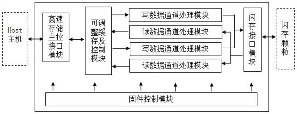
[0042] figure 1 A specific structure of a storage master control architecture in this embodiment is shown. Such as figure 1 As shown, the storage main control architecture is used to adapt to flash memory particles of different types and page capacities, including a high-speed storage main control interface module, an adjustable cache and control module, a write data channel processing module, a read data channel processing module, Flash interface module and firmware control module.
[0043] Among them, the high-speed storage main control interface module is used to receive signals from the HOST host and data to be written or read, and supports multiple storage main control interfaces with different functions, including but not limited to MMC / eMMC, SD, TF, UFS , USB interface, etc. The high-speed storage main control interface module analyzes the received information to obtain information such as high-speed data link control signals, address signals, data signals, and diffe...
Embodiment 2
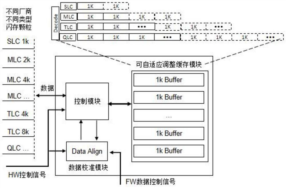
[0052] figure 2 The frame structure of the adjustable cache and control module in this application is shown. Such as figure 2 As shown, on the basis of Embodiment 1, each functional module in the adjustable cache and control module (Switch Buffer Control) includes a control module that parses input instructions and controls data processing, a data alignment module (DataAlign), and an adaptive Adjust the caching module. Wherein, the control module is used to analyze input instructions and control data processing; the data calibration module is connected to the control module; the adaptively adjustable cache module is connected to the control module, and the adaptively adjustable cache module can be divided into different capacities cache interval. The self-adaptively adjustable cache module processes various information signals and data information generated after proofreading according to the firmware program (Firmware), discriminates and decodes the flash storage particl...
Embodiment 3
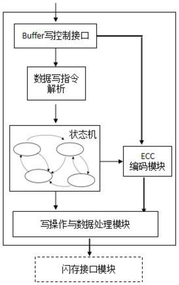
[0054] image 3 It shows the frame structure of the write data channel processing module in this application. Such as image 3 As shown, on the basis of Embodiment 1, the data channel processing module includes a Buffer write control interface module, a data write instruction analysis module, a write instruction state machine conversion and processing module, an ECC encoding module, and a write operation and data processing module. Among them, the Buffer write control interface module is connected with the adjustable cache and control module to receive the data to be written from the cache area; the data write command analysis module is used to analyze the write command; the write command state machine conversion and processing module is used to control The state machine analyzes and judges the write instruction operation, address and data information; the data error correction encoding module is used to encode the data to be written; the write operation and data processing m...
PUM
 Abstract
Description
Claims
Application Information
 - Generate Ideas
- Intellectual Property
- Life Sciences
- Materials
- Tech Scout
- Unparalleled Data Quality
- Higher Quality Content
- 60% Fewer Hallucinations
Browse by: Latest US Patents, China's latest patents, Technical Efficacy Thesaurus, Application Domain, Technology Topic, Popular Technical Reports.
© 2025 PatSnap. All rights reserved.Legal|Privacy policy|Modern Slavery Act Transparency Statement|Sitemap|About US| Contact US: help@patsnap.com