Grid-control avalanche rapid closing IGBT and symmetric structure thereof
A fast-closing, symmetrical structure technology, used in semiconductor devices, electrical components, circuits, etc., can solve the problems of too long pulse front, limit the rising speed of collector current, slow IGBT turn-on speed, etc., to shorten the pulse front and improve the pulse The effect of source performance
- Summary
- Abstract
- Description
- Claims
- Application Information
AI Technical Summary
Problems solved by technology
Method used
Image

Examples
Embodiment 1
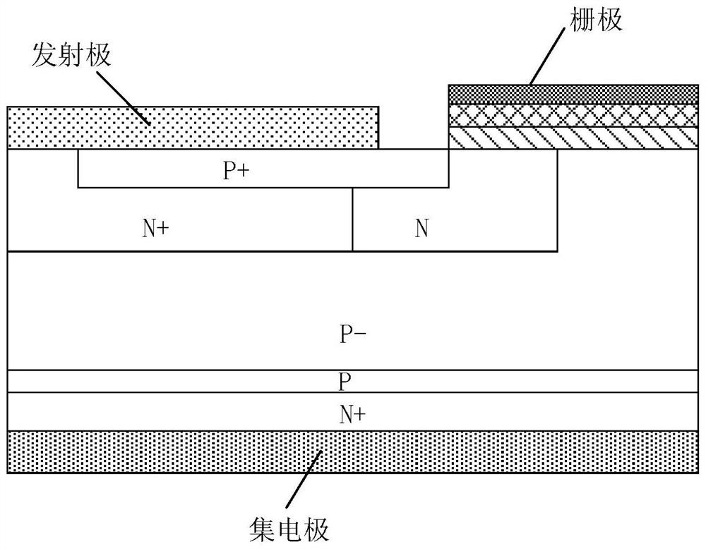
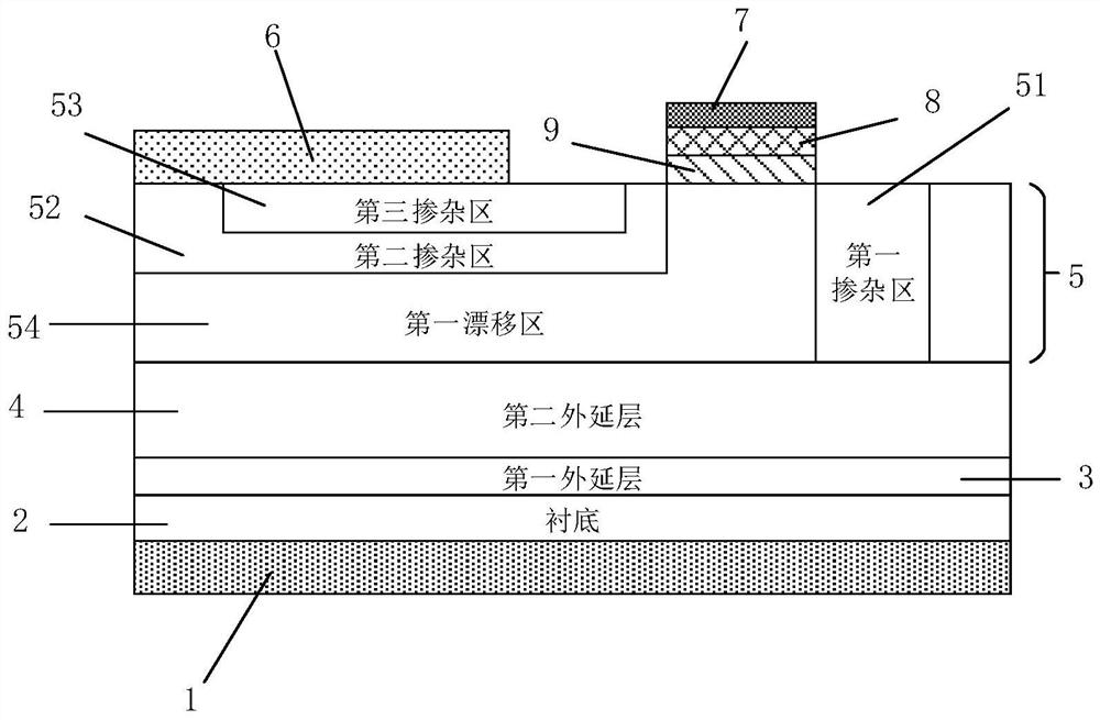
[0029] See figure 2 , figure 2 It is a schematic structural diagram of a gate-controlled avalanche fast closing IGBT provided by an embodiment of the present invention, which includes a collector metal 1, a substrate 2, a first epitaxial layer 3, a second epitaxial layer 4, and a third epitaxial layer from top to bottom 5. Emitter metal 6 and gate metal 7; wherein,
[0030] The third epitaxial layer 5 is provided with a first doped region 51, a second doped region 52 and a third doped region 53;
[0031] The first doped region 51 starts from the upper surface of the third epitaxial layer 5 and extends downward to the lower surface of the third epitaxial layer 5;
[0032] The second doped region 52 starts from the upper left corner of the third epitaxial layer 5 and extends downward and rightward to the inside of the third epitaxial layer 5 , and has a certain distance from the first doped region 51 , while forming a first drift region 54 in the part of the third epitaxial...
Embodiment 2
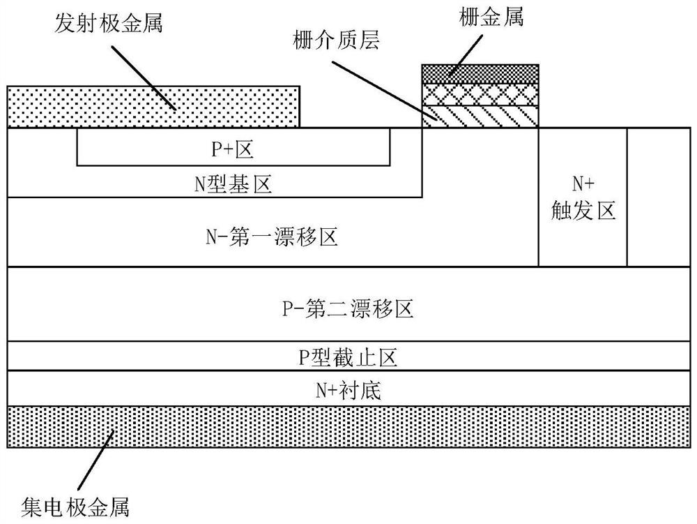
[0050] On the basis of the first embodiment above, this embodiment provides a symmetrical structure of a gate-controlled avalanche fast closing IGBT. See Figure 4 , Figure 4 It is a schematic diagram of a symmetrical structure of a gate-controlled avalanche fast-closing IGBT provided by an embodiment of the present invention, which includes the gate-controlled avalanche fast-closing IGBT provided by the first embodiment above in which two first doped regions 51 are adjacent and symmetrically arranged; A gate dielectric layer 9 , a gate 8 and a gate metal 7 are sequentially disposed above the first doped region 51 .
[0051] It can be seen that the symmetrical structure of the gate-controlled avalanche fast closing IGBT provided in this embodiment is symmetrically formed by the gate-controlled avalanche fast closing IGBT provided in the first embodiment above, and a MOS structure is also formed above the first doped region, thus This embodiment also has the advantages of th...
PUM
 Abstract
Description
Claims
Application Information