Construction method of PCB packaging model

A construction method and PCB board technology, applied in the direction of assembling printed circuits with electrical components, electrically connecting printed components, electrical components, etc., can solve the problems of increasing the overall size of terminals, failing to meet safety requirements, and unfavorable PCB layout, etc. Achieve the effects of size reduction, small space and cost saving

Pending Publication Date: 2022-04-15
清能德创电气技术(北京)有限公司
View PDF6 Cites 1 Cited by
  • Summary
  • Abstract
  • Description
  • Claims
  • Application Information

AI Technical Summary

Problems solved by technology

However, although the physical pin spacing of some high-voltage devices meets the requirements of the creepage distance, the spacing between the package pads on the PCB is too small, which makes it impossible to meet the safety requirements, which brings a lot of problems to the device selection of developers. trouble
[0004] For the case where the pin spacing of the actual device meets the requirements of the safety regulations, but the package pads cannot meet the requirements, the R&D personnel can only select another type, such as selecting a terminal with a larger pad spacing in the same series, but correspondingly, the overall size of the terminal The size will also increase. For PCB boards with limited space, the increase in terminal size is not conducive to PCB layout, and the cost will also increase

Method used


Image

  • Construction method of PCB packaging model
  • Construction method of PCB packaging model
  • Construction method of PCB packaging model

Examples


Embodiment Construction

[0031] In order to make the purpose, technical solution and advantages of the present application clearer, the present application will be further described in detail below in conjunction with the accompanying drawings and embodiments. It should be understood that the specific embodiments described here are only used to explain the present application, and are not intended to limit the present application.

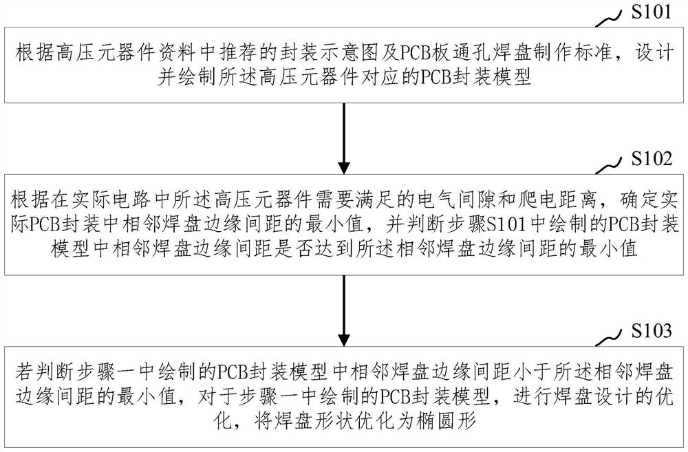
[0032] In one embodiment, such as figure 2 As shown, a method for constructing a PCB packaging model is provided, which is applied to the packaging of high-voltage components on a PCB board, and the method includes the following steps:

[0033] Step S101, designing and drawing a PCB package model corresponding to the high-voltage component according to the package schematic diagram recommended in the high-voltage component data and the PCB through-hole pad manufacturing standard;

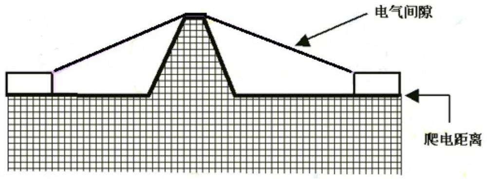
[0034] Step S102, according to the electrical clearance and creepage distance that the hig...


PUM


Abstract

The invention discloses a construction method of a PCB (Printed Circuit Board) packaging model. The method comprises the steps of designing and drawing a PCB packaging model corresponding to a high-voltage component according to a packaging schematic diagram recommended in high-voltage component data and a PCB through hole bonding pad manufacturing standard; according to the electrical gap and the creepage distance which need to be met by the high-voltage component in the actual circuit, determining the minimum value of the distance between the edges of the adjacent bonding pads in the actual PCB packaging, and judging whether the distance between the edges of the adjacent bonding pads in the drawn PCB packaging model reaches the minimum value or not; and if the result is not reached, carrying out pad design optimization on the drawn PCB packaging model, and optimizing the shape of a pad into an oval shape. According to the method provided by the invention, when the pin spacing of the high-voltage device meets the requirement of the creepage distance and the packaging bonding pad for PCB packaging does not meet the safety condition, the design of the bonding pad can be optimized according to the method provided by the invention, so that the PCB packaging model obtained after optimization can meet the requirement of the creepage distance, the through-flow can be increased, and the cost can be saved.

Description

technical field [0001] The present application relates to the technical field of circuit board packaging, in particular to a method for constructing a PCB packaging model. Background technique [0002] like figure 1 As shown, creepage distance is the shortest path between two conductive parts or between a conductive part and the protective interface of the equipment measured along the insulating surface. When designing a high-voltage and high-current power circuit board, special attention should be paid to whether the creepage distance meets the requirements, so as to ensure the safety and reliability of the circuit board and the whole device. [0003] In power conversion circuits, high-voltage devices are often used for through-hole plug-in devices and pads for in-line packages, which have the advantages of high-voltage resistance and large current flow. However, although the physical pin spacing of some high-voltage devices meets the requirements of the creepage distance...

Claims


Application Information

Patent Timeline
Patent Type & Authority Applications(China)
IPC IPC(8): H05K3/00H05K3/30H05K1/11
Inventor 张振楠刘波汤小平
Owner 清能德创电气技术(北京)有限公司
Why Eureka
Try Eureka