High-brightness surface defect detection device based on micro-lens array projection

A micro-lens array and defect detection technology, applied in the field of defect detection, can solve the problems of unclear image boundary, limited projection distance, large equipment volume, etc., and achieve the effect of reducing the company's inspection cost, improving product quality, and long projecting distance.

Pending Publication Date: 2022-04-26
慧三维智能科技(苏州)有限公司
View PDF0 Cites 0 Cited by
  • Summary
  • Abstract
  • Description
  • Claims
  • Application Information

AI Technical Summary

Problems solved by technology

Parts with highly reflective surfaces such as finely machined metals, plated and coated metals, and plastic parts have great difficulty in surface defect detection using machine vision due to strong specular reflections
[0003] The projection device used in the traditional projection method of visual inspection has disadvantages such as complex structure, large equipment volume, high power consumption of the light source, high temperature, short life, unclear image boundary, etc., and the projection distance is also limited to a certain extent.

Method used


Image

  • High-brightness surface defect detection device based on micro-lens array projection
  • High-brightness surface defect detection device based on micro-lens array projection
  • High-brightness surface defect detection device based on micro-lens array projection

Examples


Embodiment

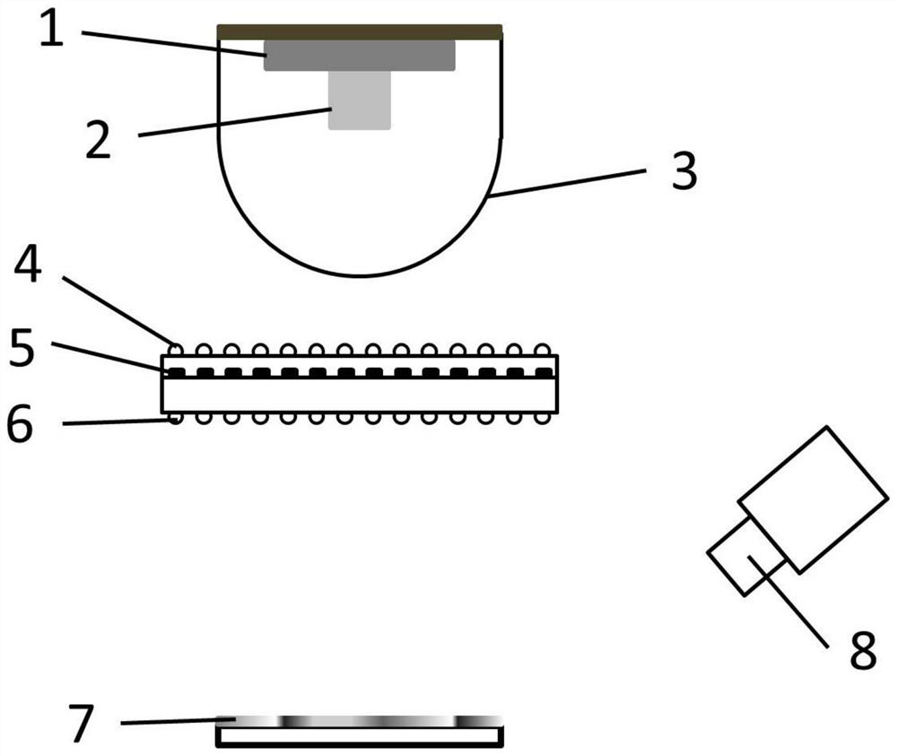
[0026] refer to figure 1 , a high-brightness surface defect detection device based on microlens array projection provided in this embodiment includes a circuit board 1, a light source 2, a collimator lens 3, a microlens array, a sample to be tested 7, and a camera 8; the light source 2 is installed on On the circuit board 1, the light source 2 is also equipped with a collimating lens 3, which can convert the scattered light emitted by the light source 2 into parallel light, and the light generated by the light source 2 is irradiated onto the sample 7 to be tested after passing through the microlens array;

[0027] The microlens array combination comprises the first microlens array 4 and the second microlens array 6 and the stripe micropattern light-shielding layer 5 between the first lens array 4 and the second lens array 6, the first microlens array 4, the stripe micro The pattern light-shielding layer 5 and the second microlens array 6 are placed in sequence along the optica...


PUM


Abstract

The invention relates to a highlight surface defect detection device based on micro-lens array projection, and relates to the field of defect detection and optics. A light source, a collimating lens and a micro-lens array are sequentially arranged along the direction of an optical axis; meanwhile, the system also comprises a sample to be detected and a camera. Stripe micro-pattern shading layers with different directions and periods can be arranged in the micro-lens array; light rays emitted by the light source pass through the collimating lens and then pass through the micro-lens array and the light shielding layer in the micro-lens array, so that different stripe pattern changes are formed on an image plane; and a stripe pattern formed by the micro-lens array covers the surface of a sample, is shot by the camera and is transmitted to visual processing software in the computer for defect detection. Compared with the prior art, the device has the advantages of simple and compact structure, uniform and clear projection pattern and high defect detection rate.

Description

technical field [0001] The invention relates to the field of defect detection, in particular to a high-brightness surface defect detection device based on microlens array projection. Background technique [0002] In modern industry, machine vision detection is widely used in the fields of working condition monitoring, product inspection and quality control. Machine vision inspection is to use the illumination source and camera to obtain the surface image of the object to be inspected. Parts with highly reflective surfaces such as finely machined metals, plated and coated metals, and plastic parts have strong specular reflections, making it difficult to detect surface defects using machine vision. [0003] The projection device used in the traditional projection method of visual inspection has disadvantages such as complex structure, large equipment volume, high power consumption of the light source, high temperature, short life, unclear image boundary, etc., and the project...

Claims


Application Information

Patent Timeline
Patent Type & Authority Applications(China)
IPC IPC(8): G01N21/88G01N21/95G03B21/00G03B21/20
CPCG01N21/8806G01N21/95G03B21/008G03B21/2006
Inventor 张翔余劲松魏凯夏勇
Owner 慧三维智能科技(苏州)有限公司
Why Eureka
Try Eureka