Semiconductor device and method for manufacturing semiconductor device

A semiconductor and device technology, which is applied in the field of semiconductor devices and semiconductor device preparation, can solve problems such as temperature effects, device performance degradation, and poor heat dissipation uniformity of devices, and achieve the effects of improving heat distribution, reducing heat accumulation, and reducing heat concentration

Active Publication Date: 2022-06-24
深圳市时代速信科技有限公司
View PDF4 Cites 0 Cited by
  • Summary
  • Abstract
  • Description
  • Claims
  • Application Information

AI Technical Summary

Problems solved by technology

In the prior art, the heat dissipation of the device is usually improved by dissipating heat from the entire active area. However, this cannot improve the heat distribution of the device, and the heat dissipation uniformity of the device is poor. For high-frequency devices, It is also prone to the problem of temperature effect leading to device performance degradation

Method used


Image

  • Semiconductor device and method for manufacturing semiconductor device
  • Semiconductor device and method for manufacturing semiconductor device
  • Semiconductor device and method for manufacturing semiconductor device

Examples


no. 1 example

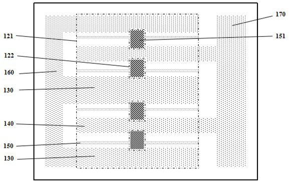
[0052] Please refer to figure 1 and figure 2 , the present embodiment provides a semiconductor device 100, which can reduce the heat accumulation in the central region of the device, reduce the heat concentration of the entire device, and improve the heat distribution of the device.

[0053] The semiconductor device 100 provided in this embodiment includes a substrate 110, a semiconductor layer 120, a source metal 130, a drain metal 140, and a gate metal 150, the semiconductor layer 120 is disposed on the substrate 110, the source metal 130, the drain The metal 140 and the gate metal 150 are disposed on the semiconductor layer 120, wherein the semiconductor layer 120 has an electrode distribution region 121, and the source metal 130, the drain metal 140 and the gate metal 150 are distributed in the electrode distribution region 121 at intervals, and A channel region is formed between the source metal 130 and the drain metal 140, the gate metal 150 is arranged in the channel ...

no. 2 example

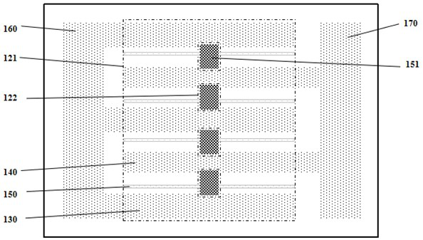
[0070] see image 3 , this embodiment provides a semiconductor device 100, the basic structure and principle and the technical effect produced are the same as those of the first embodiment. Corresponding content.

[0071] In this embodiment, the semiconductor device 100 includes a substrate 110, a semiconductor layer 120, a source metal 130, a drain metal 140 and a gate metal 150, the semiconductor layer 120 is disposed on the substrate 110, the source metal 130, the drain The metal 140 and the gate metal 150 are disposed on the semiconductor layer 120, wherein the semiconductor layer 120 has an electrode distribution region 121, and the source metal 130, the drain metal 140 and the gate metal 150 are distributed in the electrode distribution region 121 at intervals, and A channel region is formed between the source metal 130 and the drain metal 140, the gate metal 150 is arranged in the channel region, and a first isolation region 122 is arranged in the middle of the channel...

no. 3 example

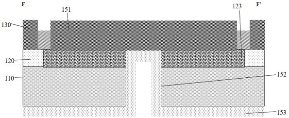
[0077] see in conjunction Figure 4 to Figure 6 , this embodiment provides a semiconductor device 100, the basic structure and principle and the technical effect produced are the same as those of the first embodiment. Corresponding content.

[0078] In this embodiment, the semiconductor device 100 includes a substrate 110, a semiconductor layer 120, a source metal 130, a drain metal 140 and a gate metal 150, the semiconductor layer 120 is disposed on the substrate 110, the source metal 130, the drain The metal 140 and the gate metal 150 are disposed on the semiconductor layer 120, wherein the semiconductor layer 120 has an electrode distribution region 121, and the source metal 130, the drain metal 140 and the gate metal 150 are distributed in the electrode distribution region 121 at intervals, and A channel region is formed between the source metal 130 and the drain metal 140, the gate metal 150 is arranged in the channel region, and a first isolation region 122 is arranged ...


PUM


Abstract

The invention provides a semiconductor device and a method for preparing the semiconductor device, and relates to the field of semiconductor technology. The semiconductor device includes a substrate, a semiconductor layer, a source metal, a drain metal and a gate metal. The source metal, the drain metal The distance between the gate metal and the gate metal is distributed in the electrode distribution area, and the gate metal is arranged in the channel region between the source metal and the drain metal, and at the same time, a first isolation region is arranged in the middle of the channel region, and the first isolation region corresponds to The semiconductor layer is a first insulating layer with insulating properties, so that a first passive heat dissipation area is formed in the first isolation area. When the device is in operation, since the first isolation region is provided with insulating properties, there will be no heat accumulation in the first isolation region due to the passage of current, and the first isolation region is located in the middle of the channel region. It can reduce the heat accumulation in the central area of ​​the device, reduce the heat concentration of the entire device, and improve the heat distribution of the device.

Description

technical field [0001] The invention relates to the technical field of semiconductors, in particular to a semiconductor device and a method for preparing the semiconductor device. Background technique [0002] The heat generated during the working process of power devices is generated and accumulated in the channel region below and near the gate. The heat distribution of the entire device is uneven, and the central area of ​​the active area (that is, the electrode distribution area) is the area where the channel is farthest from the boundary of the active area, where the temperature is the highest due to the most difficult heat dissipation, and the temperature effect causes the performance of the device to decline , The most vulnerable part of reliability failure. In the prior art, the heat dissipation of the device is usually improved by dissipating heat from the entire active area. However, this cannot improve the heat distribution of the device, and the heat dissipation ...

Claims


Application Information

Patent Timeline
Patent Type & Authority Patents(China)
IPC IPC(8): H01L23/48H01L23/488H01L21/768H01L21/60
CPCH01L23/481H01L21/76898H01L24/05H01L24/03
Inventor 许建华乐伶聪杨天应
Owner 深圳市时代速信科技有限公司
Why Eureka
Try Eureka