Semiconductor wafer silicon wafer slicing device

A technology for semiconductors and wafers, applied in the field of semiconductor wafer silicon chip slicing devices, can solve problems such as unfavorable use of slicing devices, difficult debris removal, lack of cleaning devices, etc., to improve the cleaning effect, facilitate use, and improve efficiency Improved effect

Inactive Publication Date: 2022-05-13
深圳远东卓越科技有限公司
View PDF0 Cites 0 Cited by
  • Summary
  • Abstract
  • Description
  • Claims
  • Application Information

AI Technical Summary

Problems solved by technology

[0004] The purpose of the present invention is in order to solve the shortcoming that exists in the prior art, as: can produce certain semiconductor wafer silicon chip powder and debris to remain on the semiconductor wafer silicon chip when cutting, and in existing slicing device The lack of a cleaning device makes it difficult to remove the remaining debris. It needs to be cleaned after the slicing is completed, which reduces the slicing efficiency of the device and is not conducive to the use of the slicing device. A semiconductor wafer silicon wafer is proposed Fragmentation device

Method used


Image

  • Semiconductor wafer silicon wafer slicing device
  • Semiconductor wafer silicon wafer slicing device
  • Semiconductor wafer silicon wafer slicing device

Examples


Embodiment Construction

[0018] The following will clearly and completely describe the technical solutions in the embodiments of the present invention with reference to the accompanying drawings in the embodiments of the present invention. Obviously, the described embodiments are only some, not all, embodiments of the present invention.

[0019] In describing the present invention, it should be understood that the terms "upper", "lower", "front", "rear", "left", "right", "top", "bottom", "inner", " The orientation or positional relationship indicated by "outside", etc. is based on the orientation or positional relationship shown in the drawings, and is only for the convenience of describing the present invention and simplifying the description, rather than indicating or implying that the referred device or element must have a specific orientation, so as to Specific orientation configurations and operations, therefore, are not to be construed as limitations on the invention.

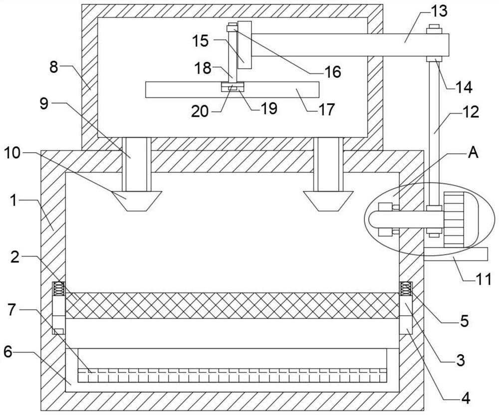
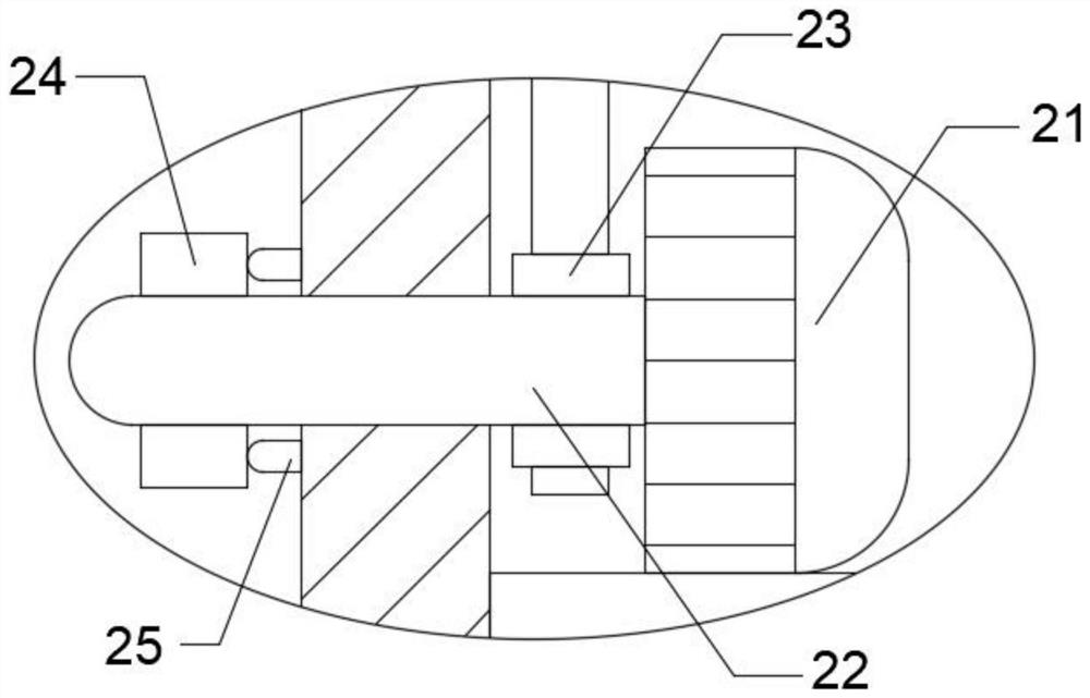
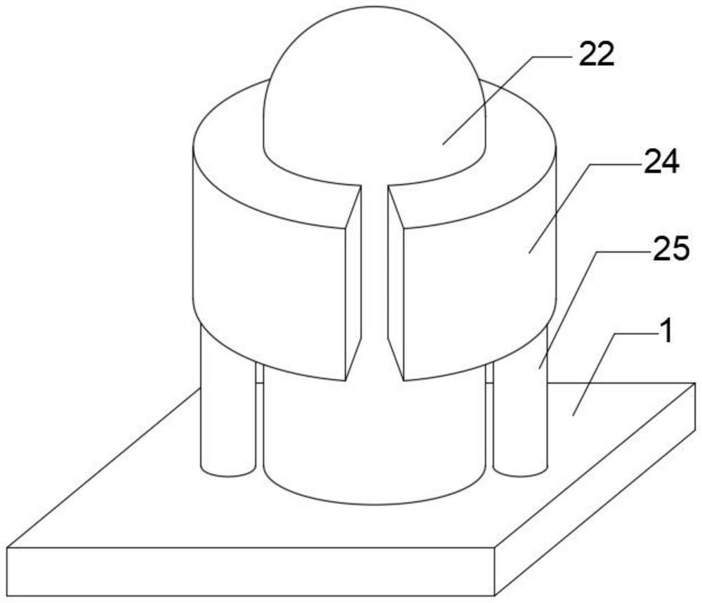
[0020] refer to Figure ...


PUM


Abstract

The invention discloses a semiconductor wafer silicon wafer separating device which comprises a flushing box, a placing grid is slidably connected in the flushing box, the left end and the right end of the placing grid are each fixedly connected with a fixed sliding block, the left inner side wall and the right inner side wall of the flushing box are each provided with a fixed sliding groove, and the left inner side wall and the right inner side wall of the flushing box are each provided with a fixed sliding block. The top end of the flushing tank is fixedly connected with a cleaning water tank, the bottom wall of the cleaning water tank is fixedly connected with a plurality of connecting pipes penetrating through the cleaning water tank, the other end of each connecting pipe is fixedly connected with a spray head, a piece separating device is arranged in the cleaning water tank, and a cleaning device is further arranged in the flushing tank. According to the slicing device, a semiconductor wafer silicon wafer can be cleaned while slicing is conducted, powder and chippings left on the semiconductor wafer silicon wafer can be cleaned away, and therefore the slicing efficiency is improved, meanwhile, the ultrasonic generation structure is further arranged, the cleaning effect can be further improved, and use of the slicing device is facilitated.

Description

technical field [0001] The invention relates to the field of semiconductor wafer silicon wafers, in particular to a semiconductor wafer silicon wafer slicing device. Background technique [0002] Wafer refers to the silicon wafer used to make silicon semiconductor circuits, and its raw material is silicon. High-purity polycrystalline silicon is dissolved and mixed with silicon crystal seeds, and then slowly pulled out to form cylindrical single crystal silicon. After the silicon ingot is ground, polished, and sliced, it forms a silicon wafer, that is, a wafer. After the wafer is prepared, it needs to be diced and cut. [0003] Most of the existing semiconductor wafer slices are cut with wire saws suitable for ultra-thin diamonds, so a certain amount of semiconductor wafer powder and debris will remain on the semiconductor wafer silicon wafers during cutting, while The existing slicing device lacks a cleaning device, and it is difficult to remove the remaining debris. There...

Claims


Application Information

Patent Timeline
Patent Type & Authority Applications(China)
IPC IPC(8): B28D5/04B28D7/00
CPCB28D5/045B28D5/0076
Inventor 蓝远东蓝远锋茹俊铭蓝远昌
Owner 深圳远东卓越科技有限公司
Why Eureka
Try Eureka