Display device and manufacturing method thereof

A technology for display devices and display areas, which can be applied to static indicators, instruments, semiconductor devices, etc., and can solve problems such as limited space

Pending Publication Date: 2022-05-20
SAMSUNG DISPLAY CO LTD
View PDF0 Cites 0 Cited by
  • Summary
  • Abstract
  • Description
  • Claims
  • Application Information

AI Technical Summary

Problems solved by technology

[0005] However, in this method, since the resistance value is adjusted only by the length of the wire, there is a problem of space limitation as the length of the wire increases

Method used


Image

  • Display device and manufacturing method thereof
  • Display device and manufacturing method thereof
  • Display device and manufacturing method thereof

Examples


Embodiment Construction

[0040] Hereinafter, a display device and a method of manufacturing the display device according to embodiments will be explained in detail with reference to the accompanying drawings. The same reference numerals are used for the same components in the drawings, and redundant descriptions of the same components will be omitted.

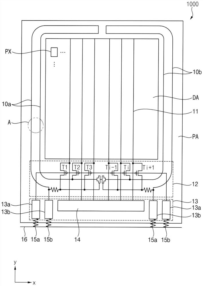
[0041] figure 1 is a plan view showing a display device according to an embodiment.

[0042] refer to figure 1 , the display device 1000 may include a display area DA and a peripheral area PA.

[0043] The display device 1000 may include a display area DA as an area where images are mainly displayed, and a peripheral area PA adjacent to the display area DA.

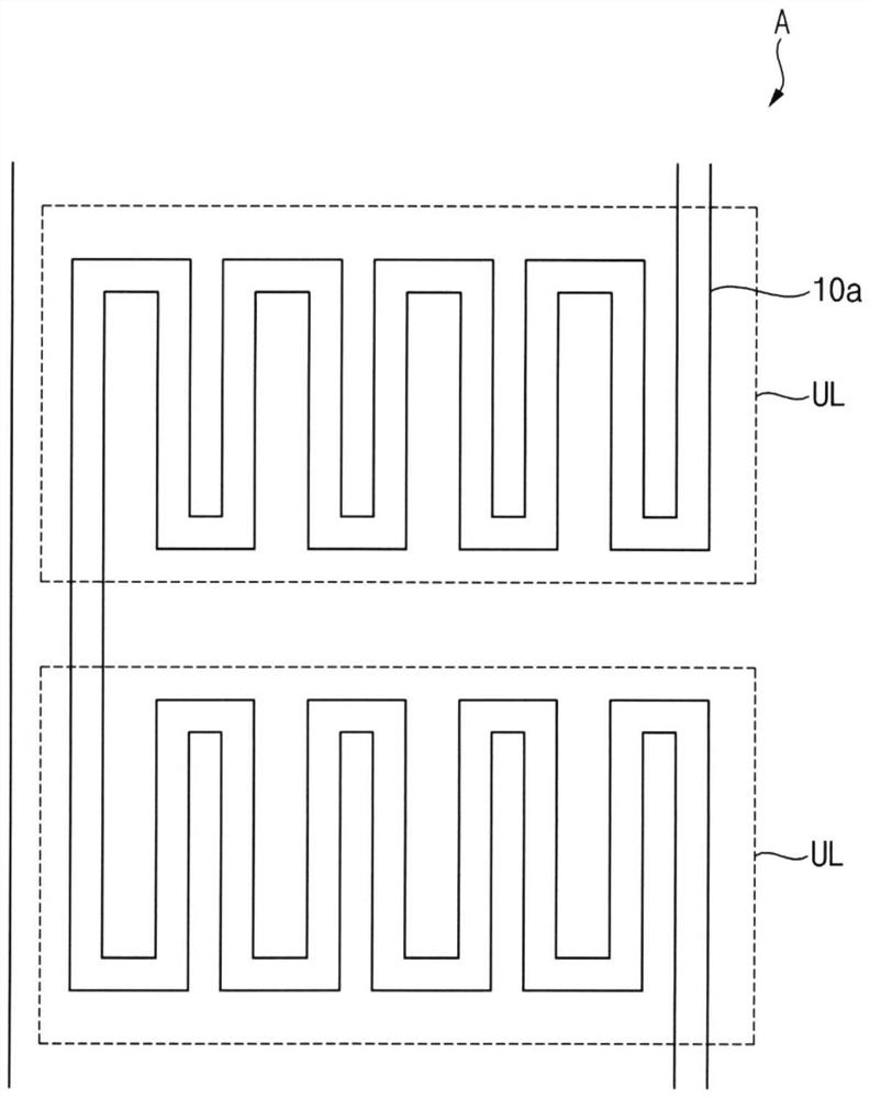
[0044] A plurality of pixels PX and a plurality of signal lines may be disposed in the display area DA. The signal lines may include a plurality of data lines 11 transmitting data signals. A plurality of data lines 11 may extend from the display area DA to the peripheral area PA along a y dir...


PUM

PropertyMeasurementUnit
electrical resistanceaaaaaaaaaa

Abstract

Disclosed are a display device and a method of manufacturing the same. The display device may include a driving transistor disposed in a display area, a test transistor disposed in a peripheral area adjacent to the display area, and a resistance line disposed in the peripheral area, electrically connected to the test transistor, and including a metal oxide.

Description

technical field [0001] The present disclosure generally relates to a display device and a method of manufacturing the same. More particularly, the present disclosure relates to a display device including a resistive wire having a metal oxide and a method of manufacturing the same. Background technique [0002] Generally, in a flat panel display device such as a liquid crystal display (LCD) or an organic light emitting display (OLED), a thin film transistor (TFT) is used as a switching element that independently drives each pixel. The thin film transistor display panel includes thin film transistors, pixel electrodes connected to the thin film transistors, gate lines for transmitting gate signals to the thin film transistors, data lines for transmitting data signals, and the like. [0003] The thin film transistor includes a gate electrode connected to a gate line, a source electrode connected to a data line, a drain electrode connected to a pixel electrode, a semiconductor ...

Claims


Application Information

Patent Timeline
Patent Type & Authority Applications(China)
IPC IPC(8): H01L27/32H01L49/02
CPCH01L28/20H10K59/12H10K59/1213H10K59/131H10K59/1201H10K59/1315H01L27/124H01L27/1225H01L27/1259G09G3/006H10K59/124
Inventor 金埈焕金允镐金兑映朴锺宇
Owner SAMSUNG DISPLAY CO LTD
Why Eureka
Try Eureka