Supercharge Your Innovation With Domain-Expert AI Agents!

Display panel and display panel manufacturing method

A technology for a display panel and a manufacturing method, which is applied in the manufacturing of semiconductor/solid-state devices, semiconductor devices, electrical components, etc., can solve the problems of complex process and the number of masks used, so as to simplify the process complexity and reduce the number of masks used. Effect

Pending Publication Date: 2022-05-27
SHENZHEN CHINA STAR OPTOELECTRONICS SEMICON DISPLAY TECH CO LTD
View PDF0 Cites 0 Cited by
  • Summary
  • Abstract
  • Description
  • Claims
  • Application Information

AI Technical Summary

Problems solved by technology

[0004] The present application provides a display panel and a display panel manufacturing method, which are used to alleviate the technical problems of using a large number of photomasks and complicated processes in the current display panel manufacturing process

Method used


Image

  • Display panel and display panel manufacturing method
  • Display panel and display panel manufacturing method
  • Display panel and display panel manufacturing method

Examples


Embodiment Construction

[0037] The technical solutions in the embodiments of the present application will be clearly and completely described below with reference to the accompanying drawings in the embodiments of the present application. Obviously, the described embodiments are only a part of the embodiments of the present application, but not all of the embodiments. Based on the embodiments in the present application, all other embodiments obtained by those skilled in the art without creative work fall within the protection scope of the present application.

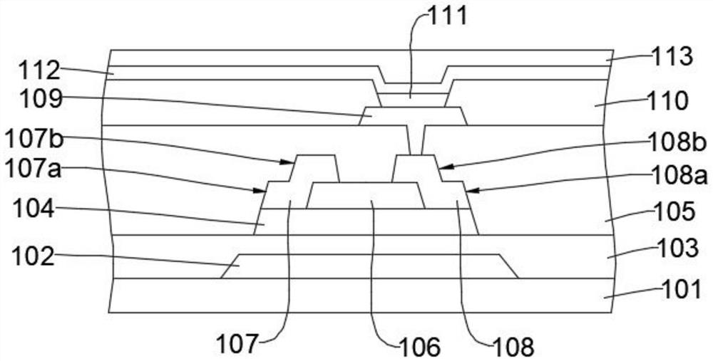
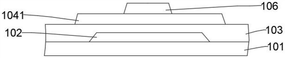
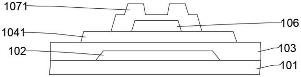
[0038] Embodiments of the present application provide a display panel and a method for fabricating the display panel. The display panel includes a driving circuit layer, and the driving circuit layer includes a semiconductor layer, and a first insulating layer and a first electrode corresponding to the semiconductor layer. The first insulating layer is disposed corresponding to the middle region of the semiconductor layer, and the first electr...


PUM


Abstract

The invention provides a display panel and a display panel manufacturing method. The display panel comprises a driving circuit layer, the driving circuit layer comprises a semiconductor layer, a first insulating layer and a first electrode layer, the first insulating layer and the first electrode layer are arranged corresponding to the semiconductor layer, and the first insulating layer is arranged corresponding to the middle area of the semiconductor layer. The first electrode layer comprises a first electrode and a second electrode which are located on the two sides of the first insulating layer respectively and arranged corresponding to the edge area of the semiconductor layer, the edge of the side, away from the first insulating layer, of the first electrode coincides with the edge of the semiconductor layer, and the edge of the side, away from the first insulating layer, of the second electrode coincides with the edge of the semiconductor layer. The edge of the first electrode and the edge of the second electrode coincide with the edge of the semiconductor layer, the number of used photomasks in the manufacturing process can be reduced, and the process complexity of the display panel is simplified.

Description

technical field [0001] The present application relates to the field of display technology, and in particular, to a display panel and a method for fabricating the display panel. Background technique [0002] In the organic light emitting diode display technology, a driving circuit layer is provided to provide power and control signals for the organic light emitting diode element, and the driving circuit layer is provided with a plurality of thin film transistor devices arranged in an array, as well as data signal lines and control signal lines. At present, in the process of preparing the driving circuit layer, it is necessary to use multiple photomask etching processes to realize the patterning treatment of the conductive film layer and the related inorganic film layer; and limited by the structural characteristics of the film layer, the current patterning operation , is to use a method of performing mask etching every time one layer of film is deposited, which results in a l...

Claims


Application Information

Patent Timeline
IPC IPC(8): H01L27/12H01L21/77H01L27/32
CPCH01L27/124H01L27/1248H01L27/1259H10K59/12
Inventor 刘方梅
Owner SHENZHEN CHINA STAR OPTOELECTRONICS SEMICON DISPLAY TECH CO LTD
Features
  • R&D
  • Intellectual Property
  • Life Sciences
  • Materials
  • Tech Scout
  • Unparalleled Data Quality
  • Higher Quality Content
  • 60% Fewer Hallucinations
Learn More