Array substrate and manufacturing method thereof
A technology of an array substrate and a manufacturing method, applied in the field of liquid crystal displays, can solve problems such as high mask cost, and achieve the effect of reducing the number of masks used and solving the high mask cost
- Summary
- Abstract
- Description
- Claims
- Application Information
AI Technical Summary
Problems solved by technology
Method used
Image

Examples
Embodiment Construction
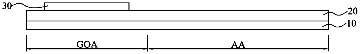
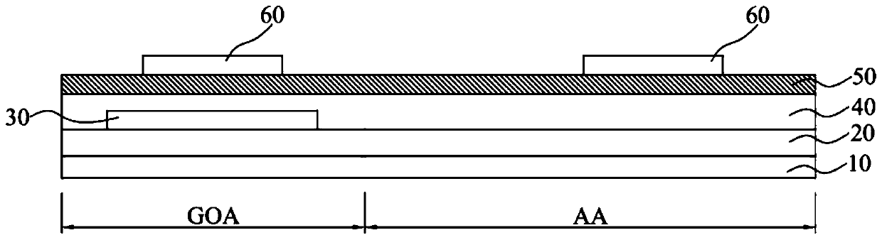
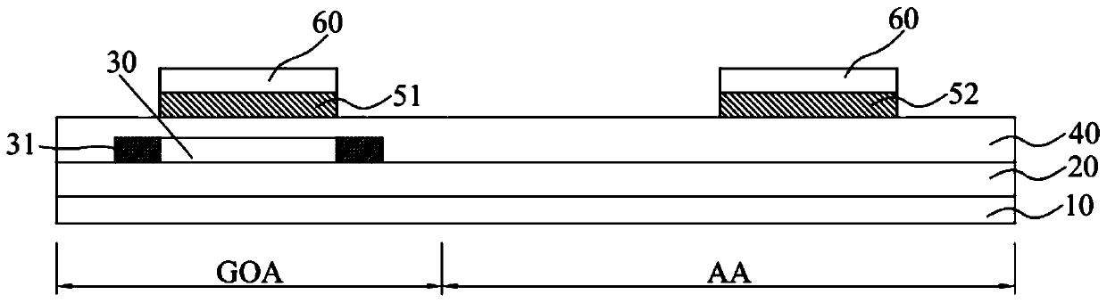
[0022] see Figure 1 to Figure 12 , the first embodiment of the present disclosure provides a method for manufacturing an array substrate 1000, which includes steps S1-S20.
[0023] Step S1: Provide a substrate 10, wherein the substrate 10 includes a display area AA and a gate driver circuit area GOA surrounding the display area AA (see figure 1 ). The substrate 10 can be a transparent substrate. The substrate 10 can be made of non-metallic materials such as glass, quartz and transparent resin with certain firmness and light guide.
[0024] Step S2: coating a buffer layer 20 on the substrate 10 (please refer to figure 1 ). The buffer layer 20 may be composed of SiOx, SiNx or a combination thereof.
[0025] Step S3: Form a polysilicon layer 30 on the buffer layer 20 in the gate drive circuit area GOA (please refer to figure 1 ). This step includes: forming an amorphous silicon layer on the buffer layer 20 , performing crystallization treatment by laser annealing to for...
PUM
 Abstract
Description
Claims
Application Information