Chip packaging pin distribution method and device, electronic equipment and storage medium

A chip packaging and chip tube technology, applied in electrical digital data processing, computer-aided design, instruments, etc., can solve the problems of cumbersome and error-prone allocation work, and achieve the effect of improving development efficiency, reducing errors and omissions, and saving labor costs.

Pending Publication Date: 2022-05-31
集睿致远(厦门)科技有限公司
View PDF0 Cites 0 Cited by
  • Summary
  • Abstract
  • Description
  • Claims
  • Application Information

AI Technical Summary

Problems solved by technology

[0004] Based on the cumbersome and error-prone problem of chip package pin allocation, the present invention provides a chip package pin allocation method, device, electronic equipment, and storage medium, which can manage chip pin connection relationships in a more intuitive and simple manner, saving Labor cost

Method used


Image

  • Chip packaging pin distribution method and device, electronic equipment and storage medium
  • Chip packaging pin distribution method and device, electronic equipment and storage medium
  • Chip packaging pin distribution method and device, electronic equipment and storage medium

Examples


Embodiment Construction

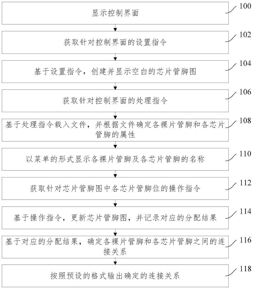
[0046] In order to make the purpose, technical solutions and advantages of the embodiments of the present invention clearer, the technical solutions in the embodiments of the present invention will be clearly and completely described below in conjunction with the drawings in the embodiments of the present invention. Obviously, the described embodiments It is a part of the embodiments of the present invention, but not all of them. Based on the embodiments of the present invention, all other embodiments obtained by those of ordinary skill in the art without creative work belong to the protection of the present invention. scope.

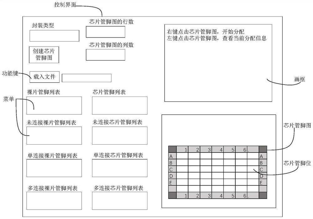
[0047] As mentioned above, in actual engineering, in order to realize chip package pin allocation, chip designers need to provide package designers with documents (such as Excel, etc.) to describe the connection relationship between the bare chip pins and chip pins (ie pad-pin mapping relationship), and sometimes it is necessary to give a chip pin diagr...


PUM


Abstract

The invention relates to the technical field of semiconductor manufacturing, in particular to a chip packaging pin distribution method and device, electronic equipment and a storage medium, and the method comprises the steps: displaying a control interface; acquiring a setting instruction for the control interface; based on the setting instruction, creating and displaying a blank chip pin diagram; acquiring a processing instruction for the control interface; loading a file based on the processing instruction, and determining attributes of each bare chip pin and each chip pin according to the file; displaying the names of the bare chip pins and the chip pins in a menu form; obtaining an operation instruction for each chip pin position in the chip pin diagram; updating the chip pin diagram based on the operation instruction, and recording a corresponding distribution result; determining a connection relationship between each bare chip pin and each chip pin based on the corresponding distribution result; and outputting the determined connection relationship according to a preset format. According to the invention, the chip pin connection relationship can be managed in a more intuitive and simple manner, and the labor cost is saved.

Description

technical field [0001] Embodiments of the present invention relate to the technical field of semiconductor manufacturing, and in particular to a chip package pin assignment method, device, electronic equipment, and storage medium. Background technique [0002] Package (Package) is the process of assembling an integrated circuit die (Die) into a chip. It is necessary to place the integrated circuit die (Die) on a substrate that acts as a load bearing, and then lead the die pin (pad) out of the package. Get the chip pins (pins) available for connection. [0003] At present, in order to realize chip package pin allocation, chip designers need to provide package designers with the connection relationship between bare chip pins and chip pins, and sometimes need to provide chip pin maps for package designers refer to. Because there are often a large number of chip pins, when chip designers assign chip package pins, the work is cumbersome and repetitive, which is easy to introduc...

Claims


Application Information

Patent Timeline
IPC IPC(8): G06F30/12G06F30/392G06F30/398G06F119/18G06F113/18
CPCG06F30/12G06F30/392G06F30/398G06F2119/18G06F2113/18Y02P90/30
Inventor 崔玥
Owner 集睿致远(厦门)科技有限公司
Why Eureka
Try Eureka