Web-based chip testing and debugging system

A debugging system and chip testing technology, which is applied in error detection/correction, instrumentation, computing, etc., can solve the problems that chip testing and debugging systems cannot realize remote debugging, etc.

Pending Publication Date: 2022-06-03
管芯微技术(上海)有限公司
View PDF0 Cites 0 Cited by
  • Summary
  • Abstract
  • Description
  • Claims
  • Application Information

AI Technical Summary

Problems solved by technology

[0010] The technical problem to be solved by the present invention is to provide a web-based chip testing and debugging system to solve the problem that the existing chip testing and debugging system cannot realize remote debugging

Method used


Image

  • Web-based chip testing and debugging system
  • Web-based chip testing and debugging system
  • Web-based chip testing and debugging system

Examples


Embodiment Construction

[0026] The present invention will be further described below with reference to the accompanying drawings and embodiments.

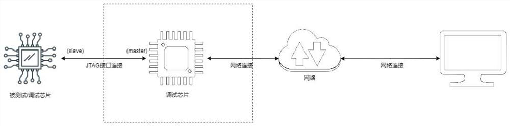
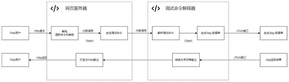
[0027] figure 2 is the Web-based chip testing and debugging system architecture in the embodiment of the present invention; image 3 It is a schematic diagram of data exchange of a Web-based chip testing and debugging system in an embodiment of the present invention.

[0028] See figure 2 and image 3 , The Web-based chip testing and debugging system of the embodiment of the present invention includes a debugging chip, the debugging chip is connected to the tested chip, the debugging chip is connected to a web browser through a network, and the Http request is sent to the debugging chip through the Web browser; the debugging chip receives Parse the Http request sent by the web browser, the debug chip parses the Http request and converts it into a JTAG command and sends it to the chip under test, the chip under test executes the JTAG command and retur...


PUM


Abstract

The invention discloses a Web-based chip testing and debugging system which comprises a debugging chip, the debugging chip is connected with a tested chip, the debugging chip is connected to a Web browser through a network, and an Http request is sent to the debugging chip through the Web browser; the debugging chip receives and analyzes an Http request sent by the Web browser, the debugging chip analyzes the Http request, converts the Http request into a JTAG command and sends the JTAG command to the tested chip, the tested chip executes the JTAG command and returns an execution result to the debugging chip, and the debugging chip converts the execution result into an Html format and sends the Html format to a network, and the Html format is checked through the Web browser. According to the invention, the Web browser is connected with the debugging chip through the network to realize remote debugging, unification of JTAG test binary codes and test commands of test chips of various models is realized, and the method is suitable for testing chips of various types.

Description

technical field [0001] The invention relates to the field of chip debugging, in particular to a Web-based chip testing and debugging system. Background technique [0002] The test of the chip refers to the process that the chip generates test incentives internally or sends test incentives to the chip through the external interface after the production is completed, and judges whether the function of the chip is correct or not by observing the internal and external operating states of the chip. Debugging refers to the process of locating hardware or software errors by running the software in real time and observing the operating state of the chip. [0003] The JTAG interface (Joint Test Action Group) is an international standard test protocol (compliant with IEEE 1149.1), and is the most commonly used interface for chip testing and software and hardware debugging. [0004] Existing chip testing and debugging systems usually consist of debuggers and debugging platforms, such ...

Claims


Application Information

Patent Timeline
Patent Type & Authority Applications(China)
IPC IPC(8): G06F11/263G06F11/273
CPCG06F11/263G06F11/273
Inventor 张欢
Owner 管芯微技术(上海)有限公司
Why Eureka
Try Eureka