
Integrated circuit with embedded memory module

A technology for memory modules and integrated circuits, applied in static memory, instruments, measurement circuits, etc., can solve problems such as reducing IC performance and affecting the function of scan test timing paths, reducing the number of switching times and avoiding power problems.

Pending Publication Date: 2022-06-24
NXP USA INC
View PDF0 Cites 0 Cited by
  • Summary
  • Abstract
  • Description
  • Claims
  • Application Information

AI Technical Summary

Problems solved by technology

However, such solutions may require additional hardware or may degrade the performance of the IC and may affect the functionality of the scan test timing path

Method used


Image

  • Integrated circuit with embedded memory module
  • Integrated circuit with embedded memory module
  • Integrated circuit with embedded memory module

Examples


Embodiment Construction

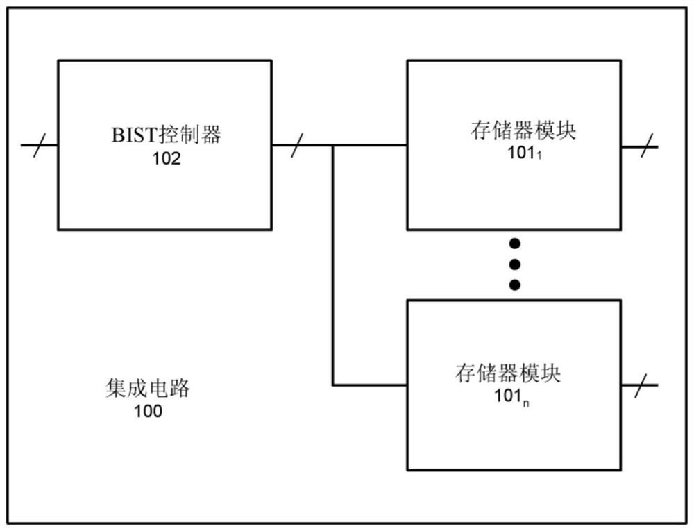
[0033] figure 1 Shown with multiple memory modules 101 1-n An example integrated circuit (IC) 100 . not for clarity figure 1 Other components shown in can also be present in IC 100 . Memory module 101 1-n The operation of each of the built-in self-test operations is controlled by the BIST controller 102, which reports to each memory module 101 1-n A signal is provided to deactivate normal operation and actually cause it to operate under the control of the BIST controller 102 .

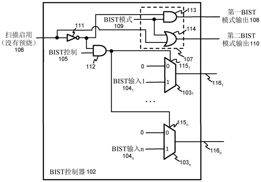
[0034] figure 2 Additional details of an example BIST controller 102 are shown. The BIST controller 102 includes: a scan enable input 106 for enabling scan shift operations; a BIST control input 105 for enabling BIST operations; a BIST mode input 109 for determining the BIST mode to be employed; Multiplexer 103 1-n BIST input for each of the 104 1-n . Each multiplexer 103 1-n Includes a pair of inputs that can be accessed by selecting input 115 1-n Enter 104 in multiple BISTs 1-n The pair...


PUM


Abstract

The present disclosure relates to a system and method for maintaining stability during scan shift operations on multiple embedded memories in an integrated circuit. Examples disclosed herein include an integrated circuit (100) including a plurality of memory modules (1011-n) and a built-in self-test (BIST) controller (102), where the BIST controller and memory modules are arranged and configured to reduce switching of cells in the memory modules during scan shift operations.

Description

technical field [0001] The present disclosure relates to a system and method for maintaining stability during scan shift operations on multiple embedded memories in an integrated circuit. Background technique [0002] An integrated circuit (IC) may include embedded memory. In some cases, particularly where larger memory capacities are required, the memory may be divided into multiple smaller memory modules distributed throughout the IC. This can reduce power consumption. However, using multiple memory modules does require the use of more boundary logic, such as a test multiplexer, for each memory address. In a scan shift operation, the normal operating mode of the IC is suspended, and multiple flip-flops in the IC are connected as long shift registers. This enables serial input test patterns to be loaded into scan chains formed from flip-flops using a single input pin. Move the result out of the scan chain and compare it to the expected result to verify that the IC is wo...

Claims


Application Information

Patent Timeline
IPC IPC(8): G01R31/3185
CPCG01R31/318555G01R31/318597G01R31/318533G11C2029/0401G11C29/32G11C29/12015G11C29/38
Inventor 杨文彬桑伟伟
Owner NXP USA INC
Learn More