Check patentability & draft patents in minutes with Patsnap Eureka AI!

Pixel structure and display panel

A technology of pixel structure and pixel group, applied in instruments, nonlinear optics, optics, etc., can solve the problem of poor display screen of the display panel, and achieve the effect of increasing the proportion

Pending Publication Date: 2022-06-24
SHENZHEN CHINA STAR OPTOELECTRONICS TECH CO LTD
View PDF13 Cites 0 Cited by
  • Summary
  • Abstract
  • Description
  • Claims
  • Application Information

AI Technical Summary

Problems solved by technology

[0005] This application provides a pixel structure and a display panel to solve the technical problem that the display panel of the current DLS architecture has a poor display picture

Method used


Image

  • Pixel structure and display panel
  • Pixel structure and display panel
  • Pixel structure and display panel

Examples


Embodiment Construction

[0040] The technical solutions in the embodiments of the present application will be clearly and completely described below with reference to the accompanying drawings in the embodiments of the present application. Obviously, the described embodiments are only a part of the embodiments of the present application, but not all of the embodiments. Based on the embodiments in the present application, all other embodiments obtained by those skilled in the art without creative work fall within the protection scope of the present application.

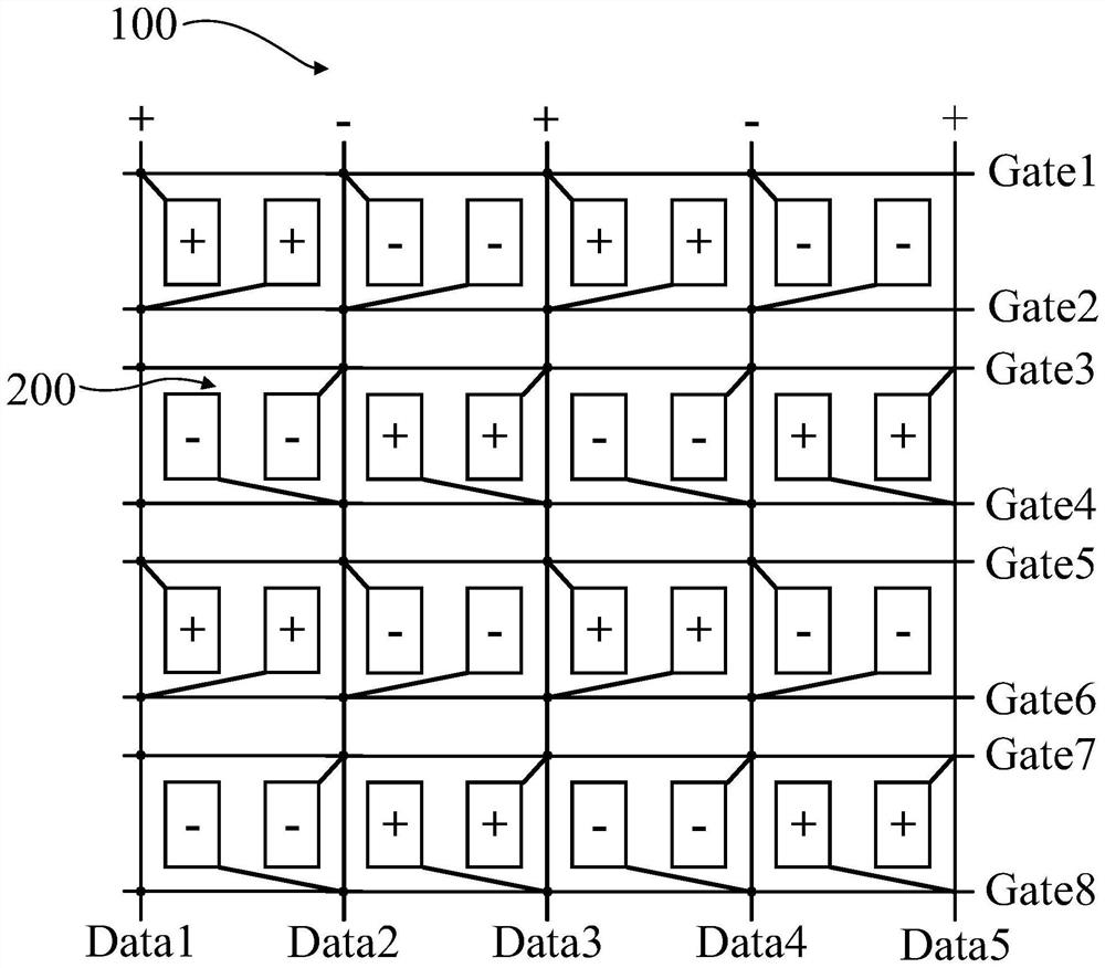
[0041] like figure 1 As shown, since two adjacent sub-pixels share a data line, Cpd1 formed by sub-pixel A and data line Data1 and Cpd2 formed by sub-pixel B and data line Data2, since there is no data line between adjacent two sub-pixels, Both Cpd1 and Cpd2 cannot be offset, resulting in the display panel's screen roughness and crosstalk being more serious than the conventional 1G1D architecture, and abnormal displays such as shaking head li...


PUM


Abstract

The invention discloses a pixel structure and a display panel. A sub-pixel group of the pixel structure comprises a common electrode, a first sub-pixel unit and a second sub-pixel unit, the first sub-pixel unit comprises a first thin film transistor, the second sub-pixel unit comprises a second thin film transistor, and a first source electrode of the first thin film transistor and a second source electrode of the second thin film transistor are connected to the same data line. The pixel structure further comprises an expansion electrode which is connected with the first drain electrode or the second drain electrode and located between the first pixel electrode and the second pixel electrode. According to the display panel, the extension electrodes are arranged between the two adjacent sub-pixel units, so that the extension electrodes and the common electrodes form new storage capacitors, the proportion of the total capacitance of the storage capacitors in the sub-pixel units is increased, the proportion of the capacitance formed by the pixel electrodes and the data lines is reduced, and the influence on a product display picture is reduced.

Description

technical field [0001] The present application relates to the field of display technology, and in particular, to a pixel structure and a display panel. Background technique [0002] LCD (Liquid Crystal Display, liquid crystal display) is currently the most widely used display product on the market, and its production technology is mature, high yield, low production cost, and high market acceptance. [0003] In the existing data line sharing (Data Line Sharing, DLS) large viewing angle pixel drive architecture display panel, the DLS architecture reduces the cost of the panel by reducing the number of source drivers (Source Drivers, SD). In the display panel of the existing DLS structure, since two adjacent sub-pixels share a data line, and no data line is provided between the two adjacent sub-pixels, the capacitors between the sub-pixels and the data line cannot be cancelled, resulting in The screen roughness and crosstalk of the display panel are more serious than those of ...

Claims


Application Information

Patent Timeline
IPC IPC(8): G02F1/1362G02F1/1368G02F1/1343
CPCG02F1/136213G02F1/1368G02F1/134309
Inventor 历杰应见见刘莹莹
Owner SHENZHEN CHINA STAR OPTOELECTRONICS TECH CO LTD
Features
  • R&D
  • Intellectual Property
  • Life Sciences
  • Materials
  • Tech Scout
  • Unparalleled Data Quality
  • Higher Quality Content
  • 60% Fewer Hallucinations
Learn More