LCD element and its making process
A technology of liquid crystal display elements and manufacturing methods, which is applied to identification devices, nonlinear optics, instruments, etc., and can solve problems such as bubbles that are easy to form vacuum areas, uneven colors, and inconsistent spacing between cells
- Summary
- Abstract
- Description
- Claims
- Application Information
AI Technical Summary
Problems solved by technology
Method used
Image
Examples
Embodiment Construction
[0050] The following is based on Figure 1(a) to Figure 6 An embodiment of the present invention will be described.
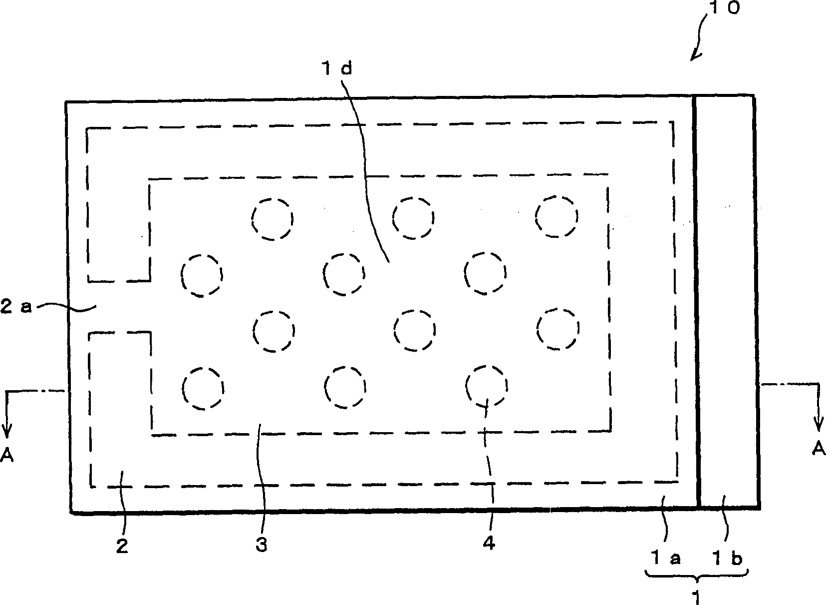
[0051] FIG. 1(a) is a plan view of the liquid crystal display element 10 of this embodiment, and FIG. 1(b) is a cross-sectional view along line A-A in FIG. 1(a). In FIG. 1( a ) and FIG. 1( b ), only the basic structural parts in the structure of the present liquid crystal display element 10 are shown. 1( a ) and FIG. 1( b ), the cell pitch (cell thickness) Cg, the spacer 4 , etc., which are gaps between the pair of substrates 1 , are enlarged for convenience of description.
[0052] As a basic structure, the present liquid crystal display element 10 has a structure including a display-side substrate 1a and a rear-side substrate 1b as a pair of substrates (upper and lower substrates) 1, and a sealing member 2 for bonding the pair of substrates 1, sandwiching The liquid crystal 3 and the spacer 4 are held between the pair of substrates 1 .
[0053] In this liq...
PUM
 Abstract
Description
Claims
Application Information


