Plastic package integrated circuit batch ultrasonic scanning inspection device and method

A technology for integrated circuits and inspection devices, which can be applied to measurement devices, analysis of solids using sonic/ultrasonic/infrasonic waves, and material analysis using sonic/ultrasonic/infrasonic waves. and other problems, to achieve the effect of improving work efficiency and accuracy, and solving the low efficiency of placing and turning over

Pending Publication Date: 2022-07-15
TECH & ENG CENT FOR SPACE UTILIZATION CHINESE ACAD OF SCI
View PDF0 Cites 0 Cited by
  • Summary
  • Abstract
  • Description
  • Claims
  • Application Information

AI Technical Summary

Problems solved by technology

The process of placing the plastic-encapsulated integrated circuit in the water on the platform in the water tank tends to drift and produce tiny bubbles that adhere to the surface of the plastic-enclosed integrated circuit. The attached micro-bubbles will affect the scanning imaging and scanning results. It is necessary to move the plastic-enclosed integrated circuit and remove the attached bubbles, resulting in The process of neatly arranging plastic-encapsulated integrated circuits is extremely difficult and inefficient
In the industry, small trays are used to arrange the plastic-encapsulated integrated circuits outside the sink, and the plastic-encapsulated integrated circuits are easy to move and cause air bubbles during the process of putting them into the sink, or use adhesive materials similar to double-sided tape on the small trays Fix the plastic-encapsulated integrated circuit, the fixed integrated circuit will not drift when it enters the water, but it will cause the adhesive to remain on the surface of the plastic-encapsulated integrated circuit
The above-mentioned various methods of placing plastic-encapsulated integrated circuits in water are time-consuming and laborious and cannot solve the problem of attached air bubbles. At the same time, plastic-enclosed integrated circuits need to scan and detect two views of the front and back, and the process of turning plastic-enclosed integrated circuits in water is time-consuming. And it is not easy to operate. The above-mentioned problems of placement and air bubbles lead to low efficiency of ultrasonic scanning of plastic-encapsulated integrated circuits

Method used


Image

  • Plastic package integrated circuit batch ultrasonic scanning inspection device and method
  • Plastic package integrated circuit batch ultrasonic scanning inspection device and method
  • Plastic package integrated circuit batch ultrasonic scanning inspection device and method

Examples


Embodiment 1

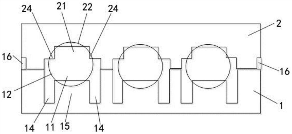
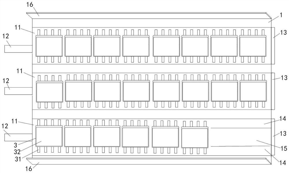
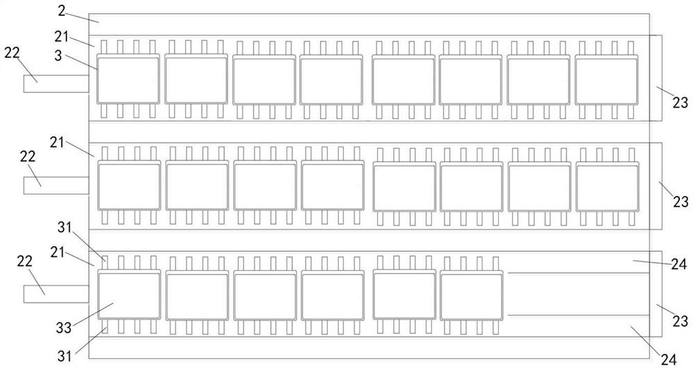
[0041] like Figure 1 to Figure 5As shown, a batch ultrasonic scanning inspection device for plastic-encapsulated integrated circuits in this embodiment includes a first tray 1 and a second tray 2, and the first tray 1 and the second tray 2 are both flat-plate structures; The tray 1 is provided with a plurality of first through grooves 11 penetrating two opposite sides of the first tray 1 . One end of the first through groove 11 is provided with a first air inlet half-pipe 12 ; the second tray 2 There are a plurality of second through grooves 21 penetrating two opposite sides of the second tray 2, and one end of the second through groove 21 is provided with a second air inlet half pipe 22; the second tray 2 can be buckled It is closed on the first tray 1, and the first through groove 11 and the second through groove 21 are enclosed to form a accommodating cavity for accommodating the plastic-encapsulated integrated circuit. The integrated circuit is stably clamped, and the fi...

Embodiment 2

[0064] A method for batch ultrasonic scanning inspection of plastic-encapsulated integrated circuits in this embodiment is implemented by using the batch ultrasonic scanning and inspection device for plastic-encapsulated integrated circuits described in Embodiment 1, and includes the following steps:

[0065]S1 , place the front surface 32 of the plastic-encapsulated integrated circuit 3 upward and continuously into the first through slot 11 of the first tray 1 , and then use the second tray 2 to buckle on the first tray 1 and closely fit the first tray 1 , put the first tray 1 and the second tray 2 into the water tank together, so that the second tray 2 is located above the first tray 1, and the front side 32 of the plastic-encapsulated integrated circuit 3 is arranged upward;

[0066] S2, use an air pump and an air tube to purge the first through groove 11 and the second through groove 21 to form the accommodation cavity for accommodating the plastic-packaged integrated circu...


PUM


Abstract

The invention relates to a plastic package integrated circuit batch ultrasonic scanning inspection device and method.The plastic package integrated circuit batch ultrasonic scanning inspection device comprises a first tray and a second tray, and the first tray and the second tray are each of a flat-plate-shaped structure; a plurality of first through grooves penetrating through the two opposite sides of the first tray are formed in the first tray, and first air inlet half pipes are arranged at notches in one ends of the first through grooves; a plurality of second through grooves penetrating through the two opposite sides of the second tray are formed in the second tray, and second air inlet half pipes are arranged at notches in one ends of the second through grooves; the second tray can be buckled on the first tray, the first through groove and the second through groove are encircled to form an accommodating cavity for accommodating a plastic package integrated circuit, and the first air inlet half pipe and the second air inlet half pipe are encircled to form an air inlet pipe. According to the invention, the problems that the efficiency of placing and turning over the plastic package integrated circuit in water in an ultrasonic scanning detection item is low and attached bubbles are difficult to remove can be solved, and the working efficiency and the accuracy of the detection work can be effectively improved.

Description

technical field [0001] The invention relates to the technical field of ultrasonic scanning and detection, in particular to a batch ultrasonic scanning inspection device and method for plastic-packaged integrated circuits. Background technique [0002] Ultrasonic scanning microscope inspection of plastic-encapsulated integrated circuits can effectively detect defects such as delamination, voids, and cracks in plastic-encapsulated integrated circuits. At present, when testing plastic-encapsulated integrated circuits in batches, the testing laboratories in the industry generally disassemble the plastic-encapsulated integrated circuits from tapes or trays and place them on the platform in the sink of the ultrasonic scanning microscope equipment. The process of placing the plastic-encapsulated integrated circuits in the water on the platform in the water tank is easy to drift and generate tiny bubbles attached to the surface of the plastic-encapsulated integrated circuits. The at...

Claims


Application Information

Patent Timeline
Patent Type & Authority Applications(China)
IPC IPC(8): G01N29/04G01N29/22G01N1/34B08B5/02B08B13/00
CPCG01N29/04G01N29/223G01N1/34B08B5/02B08B13/00
Inventor 李永正易难李昕昕孙卓午邓雪丽
Owner TECH & ENG CENT FOR SPACE UTILIZATION CHINESE ACAD OF SCI
Why Eureka
Try Eureka