
Method for protecting via holes in circuit board

A circuit board and via hole technology, which is applied in the field of protection of via holes on circuit boards, can solve insurmountable problems and achieve the effects of improving simplicity, improving pass rate, and removing accurately and effectively

Pending Publication Date: 2022-07-15
FOREWIN FPC SUZHOU
View PDF10 Cites 0 Cited by
  • Summary
  • Abstract
  • Description
  • Claims
  • Application Information

AI Technical Summary

Problems solved by technology

[0004] In order to overcome the defects in the prior art, the inventor thought of thickening the thickness of the dry film used and using a UV dry film larger than 38um to cover the via hole, but found that due to the general analysis of the UV dry film itself in the exposure process The curing ability is 35um, so it is found that even if the thickness of the UV dry film is thickened, the final analysis of the cured UV dry film is still similar to the curing effect of the previous 38um dry film, and still cannot overcome the above defects

Method used


Image

  • Method for protecting via holes in circuit board
  • Method for protecting via holes in circuit board

Examples


Embodiment Construction

[0023] The technical solutions in the embodiments of the present invention will be clearly and completely described below with reference to the accompanying drawings in the embodiments of the present invention. Obviously, the described embodiments are only a part of the embodiments of the present invention, but not all of the embodiments. Based on the embodiments of the present invention, all other embodiments obtained by those of ordinary skill in the art without creative efforts shall fall within the protection scope of the present invention.

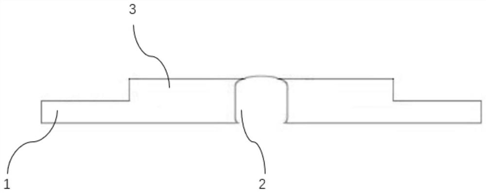
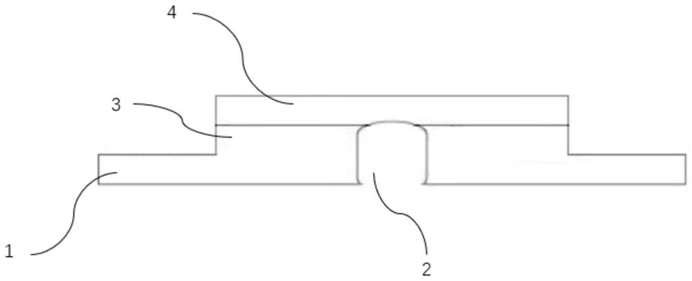
[0024] like Figure 1 to Figure 2 As shown, this embodiment provides a method for protecting a via hole on a circuit board, including the following steps:

[0025] A through hole 2 protruding from the circuit board body 1 is formed on the circuit board body 1 , and the height of the through hole 2 is between 27-35um. Therefore, the circuit board body 1 can be electrically connected through the via hole 2 subsequently. The via hole 2...


PUM


Abstract

The invention discloses a method for protecting a via hole on a circuit board. The method comprises the following steps: forming a via hole protruding out of a circuit board body on the circuit board body; covering a first UV dry film on one side of the circuit board body where the via hole is located; exposing the first UV dry film around the via hole, and removing the rest of the first UV dry film; performing film pressing treatment on the first UV dry film; covering a second UV dry film on one side of the circuit board body where the via hole is located; exposing the second UV dry film at one end, far away from the circuit board body, of the first UV dry film, and removing the rest of the second UV dry film; performing film pressing treatment on the second UV dry film; etching the circuit board body by using an etching solution; and the first UV dry film and the second UV dry film are removed. According to the invention, the etching liquid is prevented from being contacted with the via hole during etching, so that the condition of product scrapping is avoided, and the qualified rate of products is improved.

Description

technical field [0001] The invention relates to the field of circuit board processing, in particular to a method for protecting a via hole on a circuit board. Background technique [0002] The abbreviation of circuit board is PCB (Printed Circuit Board). Usually, a conductive pattern made of printed circuits, printed components or a combination of the two on the insulating material according to a predetermined design is called a printed circuit. The conductive pattern that provides electrical connection between components on an insulating substrate is called a printed circuit. In this way, the printed circuit or the finished board of the printed circuit is called a printed circuit board, also known as a printed circuit board or a printed circuit board. [0003] In actual operation, it is necessary to form a via hole protruding from the circuit board itself on the circuit board, the circuit board needs to be etched by an etching solution, and the via hole on the circuit boa...

Claims


Application Information

Patent Timeline
Patent Type & Authority Applications(China)
IPC IPC(8): H05K3/28H05K3/06
CPCH05K3/28H05K3/061H05K2203/1394
Inventor 皇甫铭徐美丽
Owner FOREWIN FPC SUZHOU
Learn More