Artificial defect graph generation and model training method and related device

A technology for artificial defects and graphics generation, applied in character and pattern recognition, instruments, calculations, etc., to achieve the effect of improving matrix generation accuracy, high similarity, and good applicability

Pending Publication Date: 2022-07-29
SEMICON MFG INT (SHANGHAI) CORP +1
View PDF0 Cites 0 Cited by
  • Summary
  • Abstract
  • Description
  • Claims
  • Application Information

AI Technical Summary

Problems solved by technology

[0007] The technical problem solved by the embodiments of the present invention is how to generate a large number of artificial defect graphics with better quality

Method used


Image

  • Artificial defect graph generation and model training method and related device
  • Artificial defect graph generation and model training method and related device
  • Artificial defect graph generation and model training method and related device

Examples


Embodiment Construction

[0023] It can be known from the background art that the number of artificial defect patterns obtained in the existing method is far from sufficient and the quality is poor.

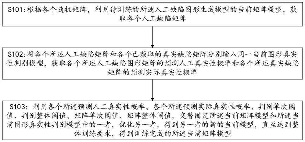
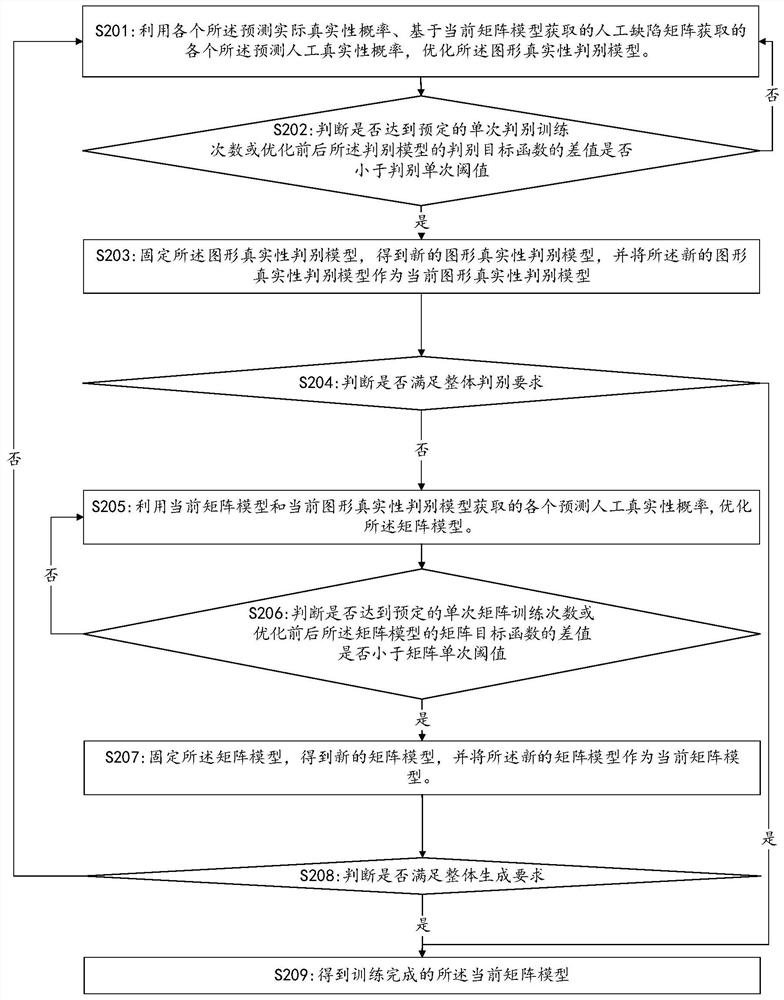
[0024] In order to solve the above problems, an embodiment of the present invention provides a training method for an artificial defect graph generation model, including:

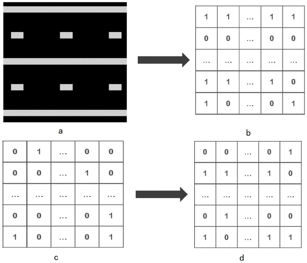
[0025] According to each random matrix, using the current matrix model of the artificial defect pattern generation model to be trained, each artificial defect matrix is ​​obtained, and the artificial defect matrix is ​​suitable for generating integrated circuit artificial defect patterns;

[0026] Input each of the artificial defect matrices and the obtained real defect matrices into the same current graphic authenticity discrimination model respectively, and obtain the predicted artificial authenticity probability of each of the artificial defect graphic matrices and the predicted actual reality of each of the real defect matrices. , ...


PUM


Abstract

The embodiment of the invention provides an artificial defect graph generation and model training method and a related device, and the provided artificial defect graph generation model training method comprises the following steps: training a matrix model of an artificial defect graph generation model and a graph authenticity discrimination model through an alternate training mode; under the condition of ensuring that the graph authenticity discrimination model has relatively high discrimination capability, the artificial defect graph generated by the matrix model of the artificial defect graph generation model is difficult to identify by the graph authenticity discrimination model, so that the matrix generation precision of the matrix model of the artificial defect graph generation model obtained by training can be improved; and a large number of artificial defect matrixes meeting quality requirements can be generated by utilizing the matrix model of the artificial defect graph generation model obtained by training.

Description

technical field [0001] Embodiments of the present invention relate to the field of semiconductors, and in particular, to a method for generating a graph, a method for training a network, and a related device. Background technique [0002] With the rapid development of semiconductor manufacturing technology, the feature size of the real graphics of integrated circuits during semiconductor processing is also decreasing, and now it has dropped to less than 10nm, and the graphics density of the real graphics of integrated circuits is also increasing. [0003] During research and development, it is inevitable that defective graphics will appear in the real graphics of integrated circuits. Finding and analyzing these defect patterns manually is difficult and time-consuming. Therefore, the model can be used to speed up the process and increase the yield. [0004] However, these models need to be trained according to corresponding defect pattern samples to find defect patterns. Ho...

Claims


Application Information

Patent Timeline
Patent Type & Authority Applications(China)
IPC IPC(8): G06V10/774G06K9/62
CPCG06F18/214
Inventor 孟阳
Owner SEMICON MFG INT (SHANGHAI) CORP
Why Eureka
Try Eureka