Formation method of semiconductor structure

A semiconductor and structure surface technology, applied in the field of semiconductor structure formation

Pending Publication Date: 2022-07-29
SEMICON MFG INT (SHANGHAI) CORP +1
View PDF0 Cites 0 Cited by
  • Summary
  • Abstract
  • Description
  • Claims
  • Application Information

AI Technical Summary

Problems solved by technology

[0004] However, the existing process of modifying a specific material as a pattern transfer mask needs to be improved

Method used


Image

  • Formation method of semiconductor structure
  • Formation method of semiconductor structure
  • Formation method of semiconductor structure

Examples


Embodiment Construction

[0024] As described in the background art, the existing process of modifying a specific material to be used as a pattern transfer mask still needs to be improved. The analysis and description will now be carried out in conjunction with specific embodiments.

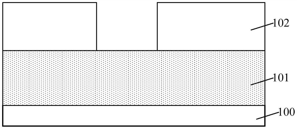
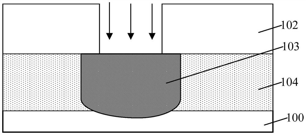
[0025] figure 1 and figure 2 It is a schematic cross-sectional structure diagram of a semiconductor structure formation process in an embodiment.

[0026] Please refer to figure 1 , providing the layer to be etched 100; forming an initial sacrificial layer 101 on the layer to be etched 100; forming a patterned layer 102 on the initial sacrificial layer 101, the patterned layer 102 exposing part of the surface of the initial sacrificial layer 101.

[0027] Please refer to figure 2 , using the patterned layer 102 as a mask to perform ion implantation on the initial sacrificial layer 101 to form a modified layer 103 and a sacrificial layer 104 .

[0028] In the semiconductor structure, the material of the initial sacr...


PUM


Abstract

The invention discloses a method for forming a semiconductor structure, which comprises the following steps of: providing a layer to be etched and an initial sacrificial layer positioned on the layer to be etched; a patterned structure is formed on the initial sacrificial layer, an opening is formed in the patterned structure, and the opening exposes part of the surface of the initial sacrificial layer; taking the patterned structure as a mask, removing a part of the initial sacrificial layer, forming a groove in the initial sacrificial layer, the depth of the groove being smaller than the thickness of the initial sacrificial layer; modifying the initial sacrificial layer on the surface of the side wall and the surface of the bottom of the groove by taking the patterned structure as a mask to form a modified layer, and enabling the initial sacrificial layer to form a sacrificial layer; after the modified layer is formed, a mask structure is formed in the groove, and the surface of the mask structure is flush with the surface of the sacrificial layer; and after the mask structure is formed, the sacrificial layer is removed, a pattern structure is formed on the to-be-etched layer, and the pattern structure comprises a modified layer and the mask structure located on the modified layer. The semiconductor structure formed by the method is good in morphology.

Description

technical field [0001] The present invention relates to the field of semiconductor manufacturing, in particular to a method for forming a semiconductor structure. Background technique [0002] In the semiconductor field, in order to obtain a semiconductor structure with multiple functions, it is necessary to design a relatively complex mask pattern for pattern transfer. In the front, middle and back stages of the semiconductor process, Self-aligned Multiple patterning (SAMP for short), Reverse Litho-Etch-Litho-Etch (Reverse Litho-Etch-Litho-Etch, A combination of one or more of RLELE) and etching processes to form various semiconductor structures that meet the needs. [0003] As the size of the semiconductor structure is further reduced, the precision of the existing photolithography technology cannot meet the dimensional accuracy requirements of the semiconductor structure. Therefore, a process of modifying a specific material as a pattern transfer mask has been introduce...

Claims


Application Information

Patent Timeline
Patent Type & Authority Applications(China)
IPC IPC(8): H01L21/027H01L21/033H01L21/308
CPCH01L21/0274H01L21/0337H01L21/0338H01L21/3086H01L21/3088
Inventor 赵猛施雪捷
Owner SEMICON MFG INT (SHANGHAI) CORP
Why Eureka
Try Eureka