

Device and method for measuring emergent mode field of optical chip
A technology of measuring device and measuring method, which is applied in the field of optical chips and can solve problems such as error and spot error
- Summary
- Abstract
- Description
- Claims
- Application Information
AI Technical Summary
Problems solved by technology
Method used
Image


Examples
Embodiment Construction
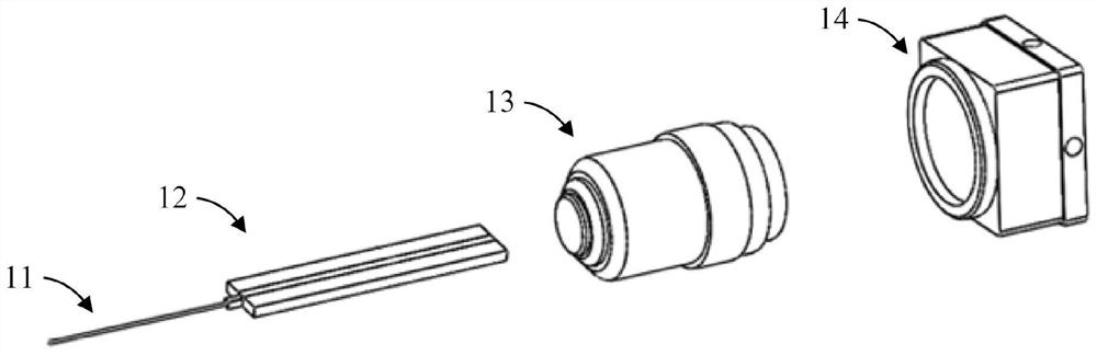
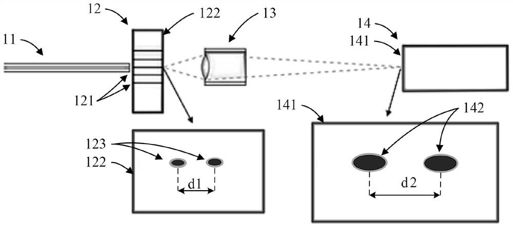
[0029] refer to figure 1 and figure 2 , the outgoing mode field measuring device for measuring the outgoing mode field of an optical chip includes a chip to be measured 12, a magnifying lens assembly 13 and a plane detector 14, the chip 12 to be measured, the magnifying lens assembly 13 and the plane detector 14 are along the optical path The directions are arranged in sequence, and the chip 12 to be measured is provided with a plurality of optical waveguides 121. In this embodiment, the optical chip adopts a parallel waveguide type optical chip, and the exit ends of the plurality of optical waveguides 121 are located on the same side and have a preset spacing d1. interval.
[0030] The magnifying lens assembly 13 includes at least one convex lens, or a lens group including a combination of convex lenses or concave lenses, so as to realize the magnification of the light spot, and the outgoing light of the plurality of optical waveguides 121 is incident on the plane detector ...
PUM
 Abstract
Description
Claims
Application Information