Device and method for measuring emergent position of optical chip

A measurement device and measurement method technology, applied in the field of optical chips, can solve the problems of inability to calculate the overlapping integral of the optical field and the electric field, increasing the overlapping integral of the optical field and the electric field, and difficulty in determining the position of the mode field, and achieve the problem of overcoming the difficulty of magnification. Effect

Active Publication Date: 2022-08-05
ZHUHAI GUANGKU TECH CO LTD
View PDF8 Cites 0 Cited by
  • Summary
  • Abstract
  • Description
  • Claims
  • Application Information

AI Technical Summary

Problems solved by technology

When designing an electro-optic modulator, in order to improve the efficiency of electro-optic modulation, it is necessary to increase the overlap integral of the optical field and the electric field as much as possible. Therefore, it is very important to determine the position of the optical waveguide mode field, especially for the optical waveguide formed by the gradient refractive index distribution. Waveguide, since the mode field in the optical waveguide and the distance between the mode field and the waveguide surface are generally on the order of a few microns, this makes it difficult to determine the position of the mode field
[0003] However, the existing measurement of the position of the mode field generally adopts an estimation method. The disadvantage of the estimation is that it is impossible to calculate the overlapping integral of the light field and the electric field, so as to accurately design the electrode.

Method used


Image

  • Device and method for measuring emergent position of optical chip

Examples


Embodiment Construction

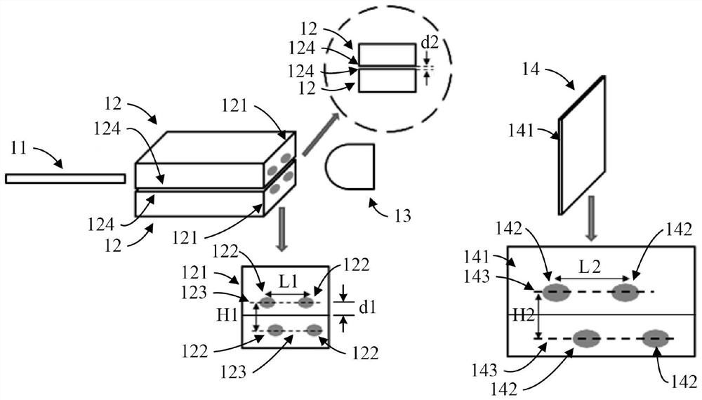
[0030] refer to figure 1 , the outgoing position determination device for determining the position of the outgoing light spot of the optical waveguide includes two chips 12 to be measured, a magnifying lens assembly 13 and a plane detector 14, and the chip 12 to be measured, the magnifying lens assembly 13 and the plane detector 14 are along the optical path. Arrange in order. The waveguide surfaces 124 of the two optical chips 12 to be measured are bonded together. The optical chips are generally arranged flat. The waveguide surface can be the surface of the optical chip. The two optical chips 12 to be measured are flatly stacked together. Glue or matching liquid can be used, and the gap S between the two waveguide surfaces 124 can be observed and measured through a microscope. In addition, the flat waveguide surfaces can be pressed together to make the gap S approach 0.

[0031] Each chip to be measured 12 is provided with at least two optical waveguides, the exit ends of t...


PUM


Abstract

The invention provides an optical chip emergent position measuring device and method, and the device comprises two to-be-measured optical chips, a magnifying lens assembly and a plane detector, each to-be-measured optical chip is provided with at least two optical waveguides, the emergent ends of the optical waveguides on the same to-be-measured optical chip are located on the same side and are spaced at a preset interval, and the plane detector is arranged on the plane detector. Waveguide surfaces of the two optical chips to be measured are attached, and emergent light of at least two optical waveguides of each optical chip to be measured is imaged and amplified by the amplification lens assembly and then enters the plane detector. Calibration is carried out according to the chip waveguide distance, the problem that the amplification factor of the lens set is difficult to calculate is solved, the trouble caused by selecting other calibration objects is also avoided, the two chips manufactured through the same technology are attached together, and the distance between light spots and the surfaces of the chips can be effectively calculated according to the distance between the emitting ends of the upper chip and the lower chip.

Description

technical field [0001] The invention relates to the field of optical chips, in particular to a device for measuring the output position of an optical chip and a method for measuring the same. Background technique [0002] Optical chip refers to a chip that uses light waves for information transmission or data operations with the help of optical waveguides, and integrates the modulation, transmission, and demodulation of optical signals and electrical signals in the same integrated optical medium. When designing an electro-optic modulator, in order to improve the efficiency of electro-optic modulation, it is necessary to maximize the overlap integral of the optical field and the electric field. For this reason, it is very important to determine the position of the optical waveguide mode field, especially for those formed by the gradient index distribution. Waveguide, because the mode field in the optical waveguide and the distance between the mode field and the surface of the...

Claims


Application Information

Patent Timeline
Patent Type & Authority Applications(China)
IPC IPC(8): G01B11/00G01M11/02
CPCG01B11/00G01M11/0242
Inventor 陆龙钊郝婷黄杭东刘昆周赤吉贵军
Owner ZHUHAI GUANGKU TECH CO LTD
Why Eureka
Try Eureka