


Quick Research
Generate reliable direction feasibility study reports for your R&D in just a few steps.

Technical Q&A
Discover and master advanced knowledge NOW. Basics, ideas, possibilities, all at once.

Find Solutions
As an expert in R&D theories, this can generate solutions to your technical problems instantly.

Evaluate Feasibility
Analyze your overall solution with one click, know your potential R&D risks in advance.

Monitor Landscape
Get weekly tech updates, stay abreast of the latest tech innovations and key insights.
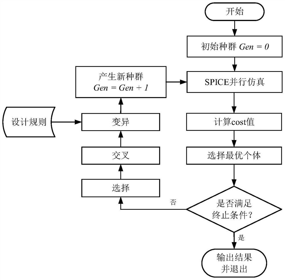
Integrated circuit optimization method and system based on rule-guided genetic algorithm
A genetic algorithm and integrated circuit technology, applied in the field of integrated circuit optimization, can solve problems such as low search efficiency, narrow topology solution space and parameter search space, and failure to meet the requirements of analog circuits, so as to save computing resources and optimize efficiency significantly , the effect of improving efficiency
- Summary
- Abstract
- Description
- Claims
- Application Information
AI Technical Summary
Problems solved by technology
Method used
Image

Examples
Embodiment 1
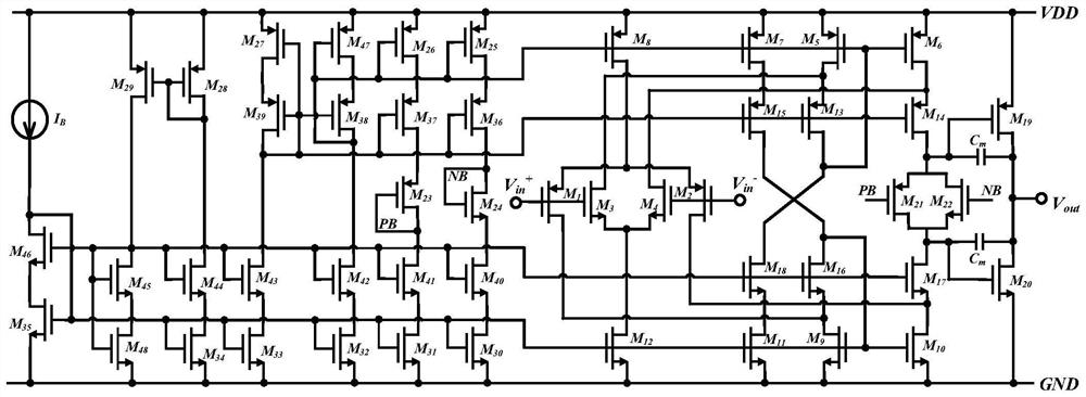
[0056] Embodiment 1 of the present invention adopts a rule-guided genetic algorithm to optimize the design of a two-level rail-to-rail operational amplifier, image 3 The circuit diagram of the two-level rail-to-rail operational amplifier described in this embodiment is realized by using a 65nm CMOS process. Table 1 lists the preset design goals of the two-stage rail-to-rail operational amplifier, that is, the circuit gain Gain, the unity gain bandwidth UGB, the phase margin PM are as large as possible, and the DC current Itot is as small as possible.
[0057] Table 1
[0058]
[0059] For this optimization goal, 13 circuit design variables to be optimized are selected, including the width W of 12 transistors 1 ,W 3 ,W 5 ,W 9 ,W 13 ,W 16 ,W 19 ,W 20 ,W 21 ,W 22 ,W 47 ,W 48 and the compensation capacitor C m . Based on current source replication and circuit symmetry, the dimensions of the other devices are as follows: M 2 The width of M and M 1 equal, that is...
Embodiment 2
[0085] Embodiment 2 of the present invention adopts a rule-guided genetic algorithm to optimize the design of a four-stage operational amplifier with a more complex topology. Figure 5 The circuit diagram of the four-stage operational amplifier described in this embodiment includes a four-stage amplifier circuit, a bias circuit, and a slew rate boost circuit (SRH). The typical application of the four-stage operational amplifier is to drive LCD, so the load capacitance to be driven is relatively large. This embodiment is implemented by a 180nm CMOS process, the power supply voltage VDD is 1.8V, and the load capacitance is 12nF. Table 3 lists the design goals of the two-stage rail-to-rail operational amplifier, namely circuit gain Gain, unity gain bandwidth UGB, phase margin PM, gain margin GM, slew rate SRr and SRf as large as possible, and DC current Itot as much as possible Small, the output node DC voltage Vout is close to VDD / 2, that is, 0.9V.
[0086] table 3
[0087] ...
Embodiment 2
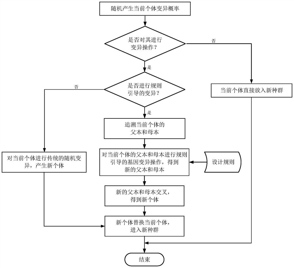
[0102] The design rule described in step 8 is defined by the user, and its implementation strategy is not unique. For Example 2, the design rules are as follows:
[0103] Rule 1, when the gain is much smaller than the design index, that is, the gain is less than 80% of the design index, it is considered that the DC operating point of the circuit deviates. The strategy adopted in this example is to adjust the DC operating point step by step according to the designer's experience, so that the amplifier tubes and load tubes of each stage are in the saturation region.
[0104] Rule 2, when the gain is slightly smaller than the design index, that is, the gain is greater than 80% of the design index but does not meet the design index, according to the circuit gain expression Gain=G m1 R O1 G m2 R o2 G m3 R O3 G m4 R O4 , where G mi (i=1,2,3,4) and R Oi (i=1, 2, 3, 4) are the equivalent transconductance and equivalent output resistance of the i-th stage, respectively. The ...
PUM
 Abstract
Description
Claims
Application Information
 - R&D Engineer
- R&D Manager
- IP Professional
- Industry Leading Data Capabilities
- Powerful AI technology
- Patent DNA Extraction
Browse by: Latest US Patents, China's latest patents, Technical Efficacy Thesaurus, Application Domain, Technology Topic, Popular Technical Reports.
© 2024 PatSnap. All rights reserved.Legal|Privacy policy|Modern Slavery Act Transparency Statement|Sitemap|About US| Contact US: help@patsnap.com