Display substrate and display device

A display substrate and sub-display technology, applied to semiconductor devices, electrical components, circuits, etc., can solve the problems of mutual damage of adjacent sub-pixel drive circuits, repair of difficult fault lines, and decrease in transparency of OLED panels, so as to reduce the difficulty of repairing dark spots and complexity, reduce the difficulty and complexity of restoration, and achieve the effect of transparent display

Pending Publication Date: 2022-08-05
HEFEI XINSHENG OPTOELECTRONICS TECH CO LTD +1
View PDF0 Cites 0 Cited by
  • Summary
  • Abstract
  • Description
  • Claims
  • Application Information

AI Technical Summary

Problems solved by technology

Since the opaque conductive layer of the anode covers the pixel drive circuit of the OLED element, it is difficult to repair the faulty circuit in the pixel drive circuit after the anode is prepared; It is also difficult to confirm defects in the anode of the photoconductive layer
[0004] In addition, in order to ensure the transparency of the transparent white OLED panel, each pixel area on the panel is usually divided into a transparent area and a pixel area (for example, each pixel area is divided into a semi-transparent area and a half-pixel area), and a pixel in the pixel area The multiple sub-pixels included are concentrated in the pixel area, which further increases the difficulty of repairing the pixel drive circuit in the pixel area, and is prone to mutual damage caused by the repair of adjacent sub-pixel drive circuits
In addition, in order to generate the repair line, metal flat lines are usually used, which will occupy the transparent area and reduce the transparency of the OLED panel

Method used


Image

  • Display substrate and display device
  • Display substrate and display device
  • Display substrate and display device

Examples


Embodiment Construction

[0060] In order for those skilled in the art to better understand the technical solutions of the present invention, a display substrate and a display device of the present invention will be described in further detail below with reference to the accompanying drawings and specific embodiments.

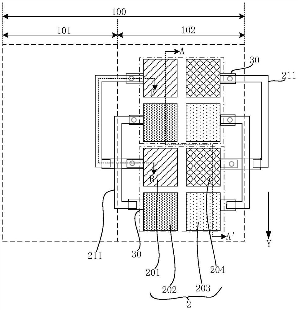
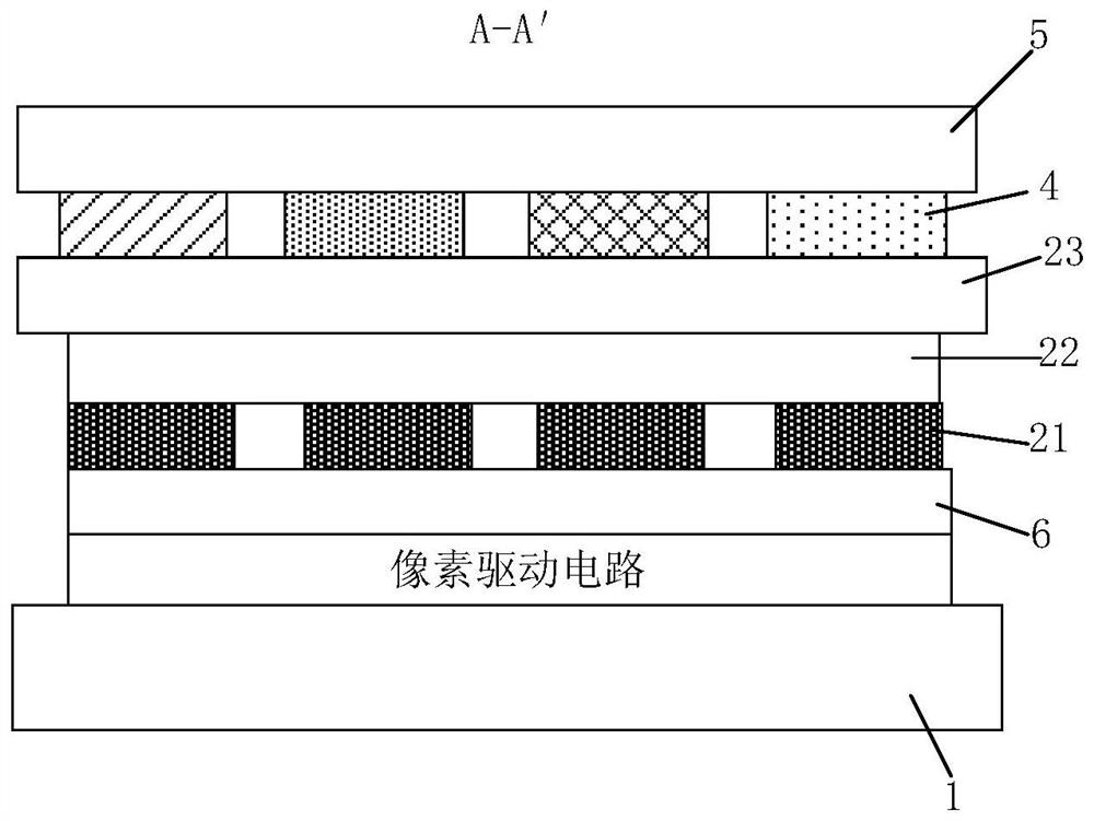
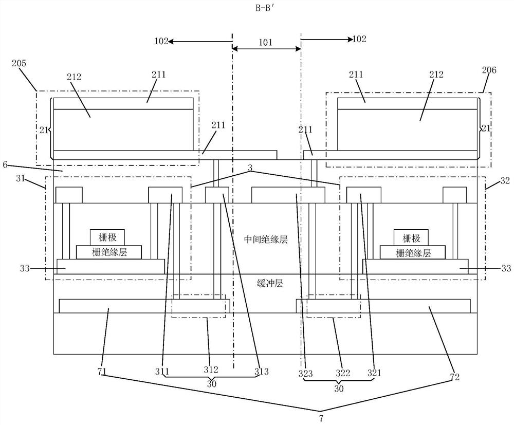
[0061] An embodiment of the present invention provides a display substrate, refer to Figure 1-Figure 3 , including a plurality of pixel regions 100; each pixel region 100 includes a transparent sub-region 101 and a display sub-region 102; the display substrate further includes a substrate 1; a plurality of light-emitting elements 2 of different colors and a plurality of pixel driving circuits are located on the substrate 1 , and is located in the display sub-area 102; a plurality of pixel driving circuits are respectively connected with a plurality of light-emitting elements 2 of different colors in a one-to-one correspondence; The light-transmitting layer 211 and the opaque layer 212 ...


PUM


Abstract

The invention provides a display substrate and a display device. The display substrate comprises a plurality of pixel regions; each pixel region comprises a transparent sub-region and a display sub-region; a substrate; a plurality of light-emitting elements with different colors and a plurality of pixel driving circuits which are located on the substrate and located in the display subarea; the plurality of pixel driving circuits are respectively connected with the plurality of light-emitting elements with different colors in a one-to-one correspondence manner; the light-emitting element comprises an anode, a light-emitting functional layer and a cathode which are sequentially stacked; the anode comprises a light-transmitting layer and a light-proof layer which are overlapped with each other; the pixel driving circuit comprises a driving tube, and a first pole of the driving tube is connected with an anode of the light-emitting element; along the first direction, in the light-emitting elements with the same color in at least two adjacent display subareas, the orthographic projection of the light-transmitting layer arranged from the display subarea to the transparent subarea and the orthographic projection of the first pole of the driving tube arranged from the display subarea to the transparent subarea on the substrate are at least partially overlapped, and the orthographic projection of the light-transmitting layer and the orthographic projection of the light-proof layer on the substrate are at least partially not overlapped.

Description

technical field [0001] The invention belongs to the field of display technology, and in particular relates to a display substrate and a display device. Background technique [0002] OLED (Organic Light-Emitting Diode, Organic Light Emitting Diode) display products have the characteristics of self-luminescence, high brightness, wide viewing angle, high contrast, flexibility, low energy consumption, etc., so they have received extensive attention and become a new generation of display methods , has begun to gradually replace the traditional LCD (Liquid Crystal Display) display products, is widely used in mobile phone screens, computer monitors, full-color TVs and so on. In the related art, OLED display panels can be classified into top emission type and bottom emission type according to their different light emission modes. [0003] Top Emission transparent WOLED Panel (ie White Organic Light-Emitting Diode Panel, namely white OLED panel) is divided into a transparent area an...

Claims


Application Information

Patent Timeline
Patent Type & Authority Applications(China)
IPC IPC(8): H01L27/32H01L51/52
CPCH10K59/351H10K59/123H10K59/121H10K50/81
Inventor 崔容豪玄丽燕胡迎宾宋嘉文赵策
Owner HEFEI XINSHENG OPTOELECTRONICS TECH CO LTD
Why Eureka
Try Eureka