Image display and method of driving image display
A technology of an image display device and a driving method, applied to image/graphic display tubes, identification devices, static indicators, etc.
- Summary
- Abstract
- Description
- Claims
- Application Information
AI Technical Summary
Problems solved by technology
Method used
Image

Examples
Embodiment 1
[0108] The image display device of Embodiment 1 of the present invention uses a display panel (display element of the present invention) on which brightness modulation elements of each dot are formed by combining a thin-film electron source matrix as an electron emission source and a phosphor, and drives a circuit It is formed by connecting to the row electrodes and column electrodes of the corresponding display panel.
[0109] Here, the display panel is composed of an electron source on which a thin film electron source matrix is formed and a fluorescent display panel on which a phosphor pattern is formed.
[0110] Image 6 It is a plan view showing a part of the structure of the thin-film electron source matrix of the electron source plate according to the embodiment of the present invention, Figure 7 is a plan view showing the positional relationship between the electron source panel and the fluorescent display panel of this embodiment.
[0111] Figure 8 It is a cros...
Embodiment 2
[0195] The display panel used in the image display device of the second embodiment of the present invention, and the connection method of the display panel and the driving circuit are the same as those of the first embodiment above.
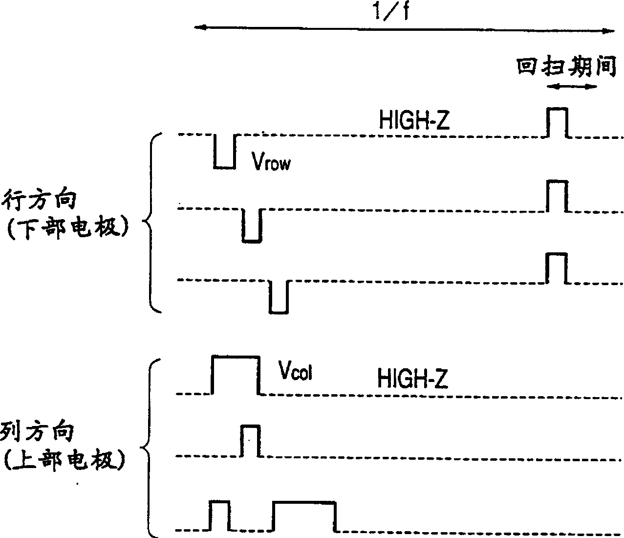
[0196] Figure 12 It is a timing chart showing an example of driving voltage waveforms output from the row electrode driving circuit 41 and the column electrode driving circuit 42 in the image display device according to the second embodiment of the present invention.
[0197] Also in this embodiment, an accelerating voltage of about 3 to 6 KV is always applied to the metal backing film 122 from the accelerating voltage source.
[0198] exist Figure 12 In , the dotted line indicates the high impedance output.
[0199] Actually, the output impedance may be about 1 to 10 MΩ, and it is 5 MΩ in this embodiment.
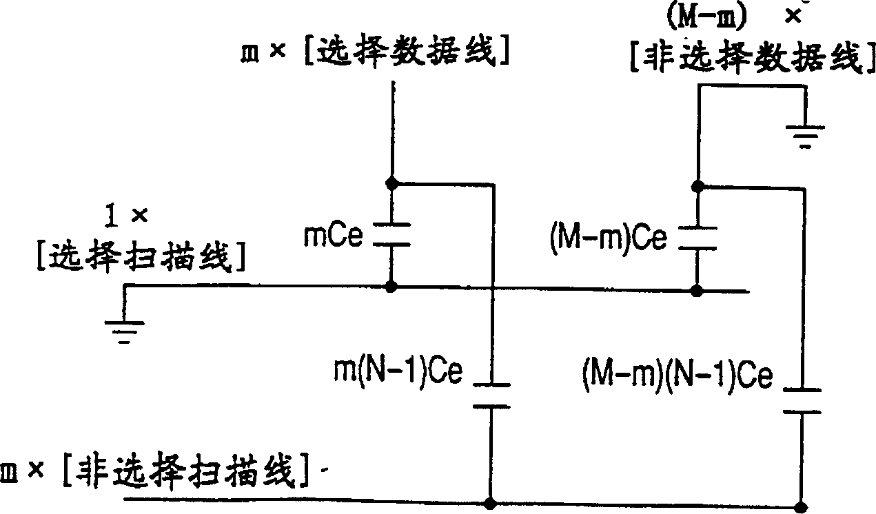
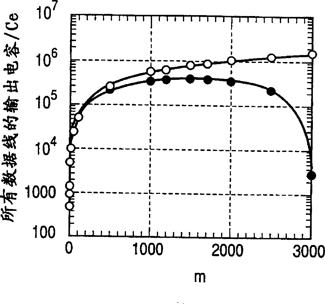
[0200] Here, as in the first embodiment, the nth row electrode 310 is represented by Rn, the mth column electrode 311 is represented by...
PUM
 Abstract
Description
Claims
Application Information
 - Generate Ideas
- Intellectual Property
- Life Sciences
- Materials
- Tech Scout
- Unparalleled Data Quality
- Higher Quality Content
- 60% Fewer Hallucinations
Browse by: Latest US Patents, China's latest patents, Technical Efficacy Thesaurus, Application Domain, Technology Topic, Popular Technical Reports.
© 2025 PatSnap. All rights reserved.Legal|Privacy policy|Modern Slavery Act Transparency Statement|Sitemap|About US| Contact US: help@patsnap.com