Electron-emitting element and electron source, field emission image display device, and fluorescent lamp utilizing the same and methods of fabricating the same

a technology of electron emission and electron source, which is applied in the manufacture of electrode systems, discharge tube main electrodes, and discharge tube/lamps. it can solve the problems of insufficient overcomement of problems, large electrical resistance, and inability to achieve smooth electron injection

Inactive Publication Date: 2005-07-05
PANASONIC CORP
View PDF14 Cites 72 Cited by
  • Summary
  • Abstract
  • Description
  • Claims
  • Application Information

AI Technical Summary

Problems solved by technology

(1) Only the very sharp tip of the tetrapod-like ZnO whisker is in contact with the graphite electrode 2202, and therefore the contact area with the electrode is very small. For this reason, when injecting electrons into the ZnO whisker, electrical resistance is very large and thus smooth electron injection is not achieved. This problem cannot be sufficiently overcome even if the surface of the ZnO whisker is coated with a low work function material.
(2) The tip of the tetrapod leg of the ZnO whisker is very sharp and has a great electric field concentration effect; at the same time, however, it is easily broken. In order to prevent whisker from breaking, whi

Method used


Image

  • Electron-emitting element and electron source, field emission image display device, and fluorescent lamp utilizing the same and methods of fabricating the same
  • Electron-emitting element and electron source, field emission image display device, and fluorescent lamp utilizing the same and methods of fabricating the same
  • Electron-emitting element and electron source, field emission image display device, and fluorescent lamp utilizing the same and methods of fabricating the same

Examples


example 1-1

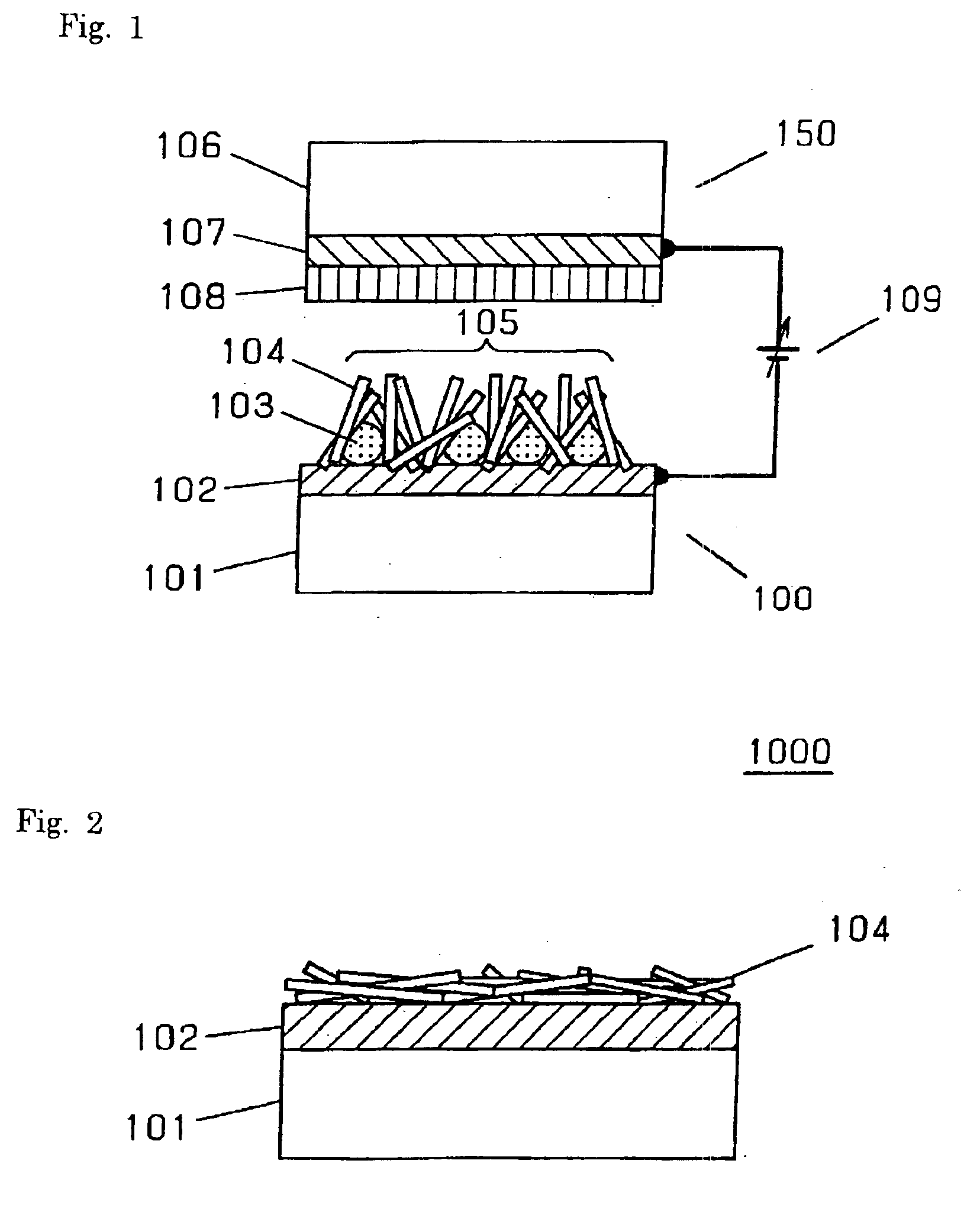
[0089]FIG. 1 is a schematic structural view of an electron-emitting element 100 according to Example 1-1 of the present invention and a field emission display device 1000 utilizing the electron-emitting element 100. Referring to FIG. 1, configurations and fabrication methods of the electron-emitting element 100 and the field emission display device 1000 are described below.

[0090]First, on a glass supporting substrate 101 serving as a support member a metal thin film serving as a first conductive electrode (conductive layer) 102, made of Al, an Al—Li alloy, Mg, an Mg—Ag alloy, Au, Pt, Ag, Fe, Ni, Cu, Cr, W, Mo, Co, Ta, Ti, or the like, was formed by sputtering, vacuum deposition, or plating, to a thickness of about 0.01 to 100 μm, typically to about 0.1 to 1 μm.

[0091]Next, a liquid having therein substantially spherical metal fine particle (particle size: 0.1 to 8 μm) made of a material such as Pt, Au, Ag, Cu, Ni, Rh, Pd, Co, a Cu—Sn alloy, a Cu—Zn alloy, a Cu—Ni—Zn alloy, a Cu—Pb a...

example 1-2

[0107]In Example 1-2 of the present invention, in accordance with the fabrication process of the electron-emitting element 100 fabricated in Example 1-1, a second particle 103 was dispersed over a first conductive electrode 102 using a spin coater. Thereafter, a stainless steel plate was pressed down on the second fine particle 103, thereby fixing the particle to the first conductive electrode 102 by applied pressure. Subsequently, carbon nanotubes serving as a first particle 104 were dispersed in the same manner as that described in Example 1-1, thus configuring an electron-emitting element. Other components and a fabrication method are the same as those described in Example 1-1, and thus description is omitted here.

[0108]The electron-emission characteristics of the present example were examined in the same manner as in Example 1-1 and the voltage at which electrons start to be emitted was approximately 10% smaller and the emission current was approximately 10% higher than those of...

example 1-3

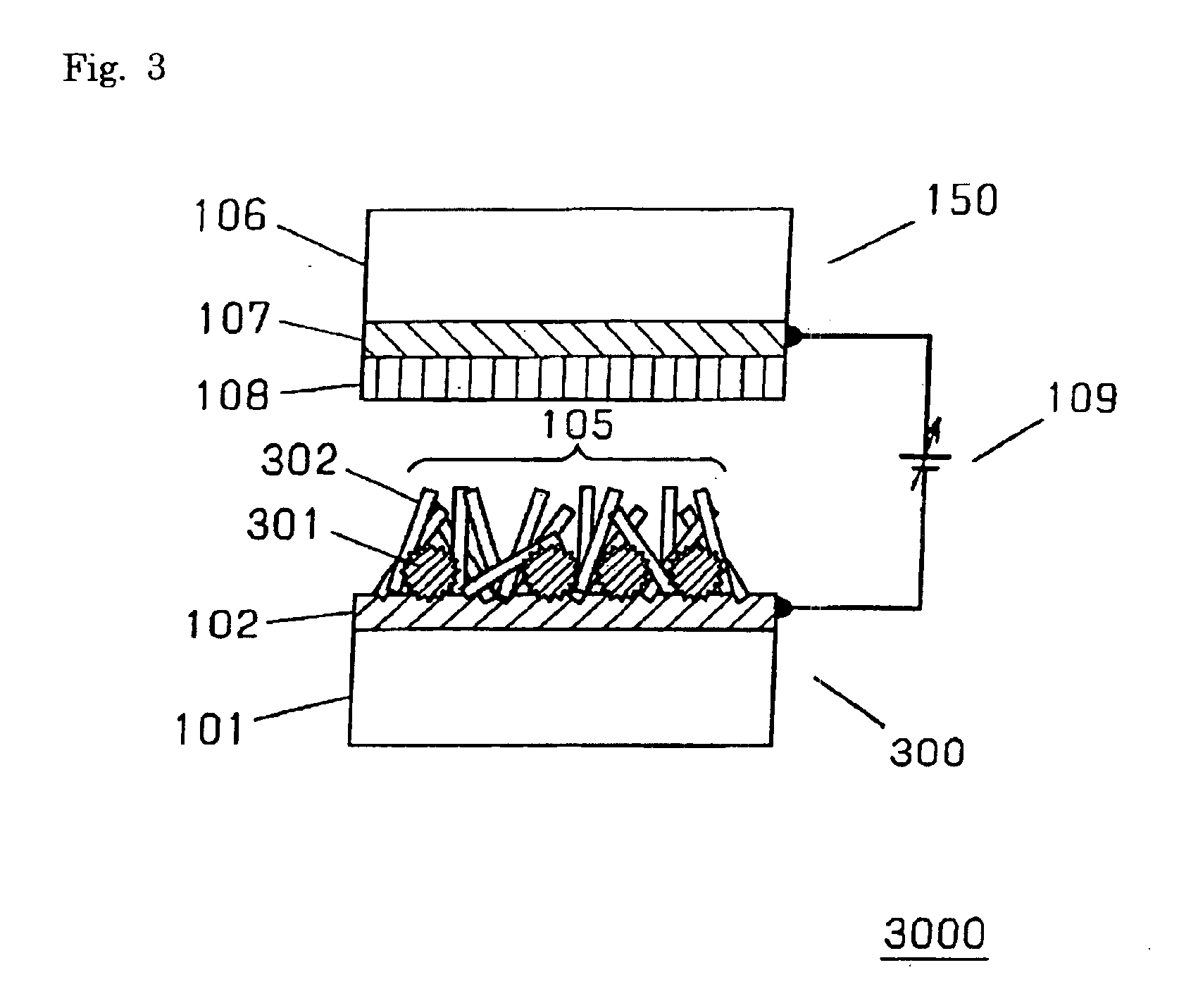
[0111]In Example 1-3 of the present invention, in accordance with the fabrication process of the electron-emitting element 100 fabricated in Example 1-1, a first particle 104 and a second particle 103 were mixed together and dispersed in a volatile organic solvent such as ethanol, isopropyl alcohol, or acetone. The dispersion was then dripped onto a first conductive electrode 102 and was allowed to dry, thereby configuring a cold cathode member 105 in which the first particle 104 and the second particle 103 were mixed together, and thus configuring an electron-emitting element. Other components and a fabrication method are the same as those described in Example 1-1, and thus description is omitted here.

[0112]The electron-emission characteristics of the present example were examined in the same manner as in Example 1-1 and substantially the same results were obtained as were with the element 100 in Example 1-1. It should be noted that Example 1-1 differs from Example 1-3 in that disp...


PUM


Abstract

Disclosed are an electron-emitting element having a large operating current at a low operating voltage and excellent operation stability, and an electron source, an image display device and the like utilizing such an electron-emitting element, and further a method of fabricating such an element with few process steps at low cost. A cold cathode member is configured utilizing hybrid particle of a first particle serving to emit electrons into the space and a second particle being in the vicinity of the first particle and serving to control the position of the first particle. In this configuration, it is preferable that the first particle have a higher electron emission efficiency than the second particle and that the second particle be conductive.

Description

TECHNICAL FIELD[0001]The present invention relates to an electron-emitting element for emitting electrons, an electron source configured utilizing such an electron-emitting element, and an image display device and a fluorescent lamp configured utilizing such an electron source, to fabrication methods thereof, and further to a method of forming a pattern that can be suitably applied to such fabrication methods. The present invention is described below in two parts: a first invention group and a second invention group.[0002](Common remarks) First, the general meaning of the term “particle” as used in this specification is described. The term “particle” as used herein means a solid that exists individually and independently and does not specify shape. Examples of shapes of the “particle” include sphere, oval, column, rod, grain, cylinder, needle, tetrapod, and plate, and in a case where shape needs to be specified, a term that describes the shape, for example, such as “fiber-like parti...

Claims


Application Information

Patent Timeline
IPC IPC(8): H01J63/00H01J63/06H01J1/304H01J1/30H01J9/02
CPCB82Y10/00H01J1/3048H01J9/025H01J63/06H01J2201/30403H01J2201/30469Y10S977/939B82Y40/00C01B32/05H01J1/304H01J9/02
Inventor AKIYAMA, KOJISHIRATORI, TETSUYAKUROKAWA, HIDEOKAWASE, TORU
Owner PANASONIC CORP
Why Eureka
Try Eureka