Testing apparatus using charged particles and device manufacturing method using the testing apparatus

An electron beam device and electron beam technology, applied in the field of device manufacturing

Inactive Publication Date: 2006-08-16
EBARA CORP
View PDF0 Cites 67 Cited by
  • Summary
  • Abstract
  • Description
  • Claims
  • Application Information

AI Technical Summary

Problems solved by technology

[0008] In the SEM method inspection device described above, it can be considered that the above-mentioned inspection speed is almost the limit, and in order to further increase the speed, that is, increase productivity, a new method is required.

Method used


Image

  • Testing apparatus using charged particles and device manufacturing method using the testing apparatus
  • Testing apparatus using charged particles and device manufacturing method using the testing apparatus
  • Testing apparatus using charged particles and device manufacturing method using the testing apparatus

Examples


Embodiment approach

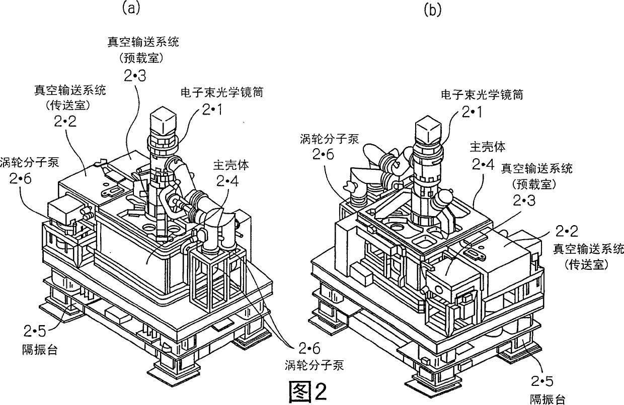
[0215] 2-1) Conveying system

[0216] 2-1-1) Box stand

[0217] 2-1-2) Microenvironment device

[0218] 2-1-3) Main shell

[0219] 2-1-4) Loader housing

[0220] 2-1-5) Loader

[0221] 2-1-6) Workbench device

[0222] 2-1-7) Chip clamping mechanism

[0223] 2-1-7-1) Basic structure of electrostatic chuck

[0224] 2-1-7-2) Clamping mechanism for 200 / 300 bridging tools

[0225] 2-1-7-3) Chip clamping process

[0226] 2-1-8) Device structure for 200 / 300 bridging tool

[0227] 2-2) How to transport wafers

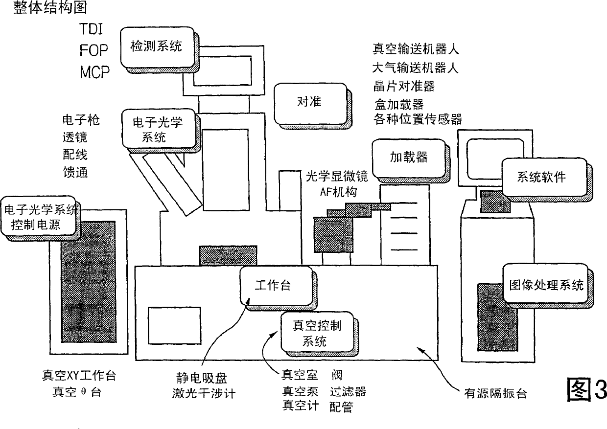
[0228] 2-3) Electron optical system

[0229] 2-3-1) Summary

[0230] 2-3-2) Details of the structure

[0231] 2-3-2-1) Electron gun (electron beam source)

[0232] 2-3-2-2) Primary optical system

[0233] 2-3-2-3) Secondary optical system

[0234] 2-3-3) E×B unit (Wien filter)

[0235] 2-3-4) Detector

[0236] 2-3-5) Power

[0237] 2-4) Pre-charging unit

[0238] 2-5) Vacuum exhaust system

[0239] 2-6) Control system

[0240] 2-6-1) Structure and function

[0241] 2-6-2) Alignment ...

Embodiment approach 1

[0464] This is an example of an inspection device mainly composed of a vacuum chamber, a vacuum exhaust system, a primary optical system, a secondary optical system, a detector, an image processor, and a control computer. Fig. 26 shows an example of this.

[0465] It has a primary optical system 26·1 for irradiating an electron beam onto a sample and a secondary optics for guiding electrons emitted from the surface of the sample, such as secondary electrons, reflected electrons, backscattered electrons, etc., to the detector System 26·2. The secondary optical system is a projection type optical system. In order to separate the primary system and the secondary system, a so-called E×B beam splitter 26·3 is used. In addition, the electronic image signal detected by the detector 26·4 is converted into an optical signal or / and an electrical signal, and processed by the image processor 26·5. At this time, even if the number of electrons incident on the detector is 200 or less in an area...

Embodiment approach 2

[0520] In the same inspection device as in the first embodiment, when the detector adopts a TDI sensor / camera, if the number of pixels / stages is 2048 or more and 4096 or less, and the number of taps is 32 or more and 128 or less, the sensitivity is 10000-40000DN / ( nJ / cm 2 ), it is possible to obtain images at a higher speed and efficiency. At this time, the line frequency can use 100-400kHz, and the video rate can use 10MHz-40MHz. At this time, when an 8-inch Si wafer, such as an LSI device wafer, has a resolution of 0.1 μm / pixel, the inspection time per wafer can be performed in 1 / 8 to 2 hours.

[0521] At this time, when the resolution is 0.1μm / pixel, in sample observation and defect inspection, for example, when the pattern shape is L / S: 0.2 / 0.2μm, the contrast ratio can be 3-30%, which is enough for image observation. And defect detection. For defects of shapes other than L / S, the comparison is made by the change of the ratio, and it can be detected if the size is 1 pixel or m...


PUM

PropertyMeasurementUnit
diameteraaaaaaaaaa
surface smoothnessaaaaaaaaaa
diameteraaaaaaaaaa

Abstract

The invention provides a method for further increasing an inspection speed, i.e. increasing the productivity of the inspection device in an SEM manner. The inspection device which inspects the surface of a substrate images in the direction of a sample W with expected times to form crossover after an electron generated from an electron source (25*1) forms crossover. When allowing the crossover to pass through, an electron as noise is removed from an opening, the crossover is set to be expected times and adjusted to be parallel electron beams to irradiate a substrate with a desired sectional shape. The electron beam is adjusted so as to keep unevenness in electron beam illumination intensity to up to 10%. Electrons emitted from the sample W are detected by a detector (25*11).

Description

Technical field [0001] The present invention relates to an inspection device that uses electron beams to inspect defects in patterns formed on the surface of an inspection object, and more specifically, relates to irradiating an inspection object with electron beams as in the case of inspecting wafer defects in a semiconductor manufacturing process An inspection device that captures and captures secondary electrons that vary in accordance with the performance of its surface to form image data, and inspects patterns and the like formed on the surface of the inspection object based on the image data with high productivity, and uses this inspection device to A device manufacturing method for manufacturing devices with high yield. More specifically, it relates to a detection device using a surface beam image projection method and a device manufacturing method using the device. [0002] In the semiconductor process, design rules will usher in the 100nm era, and the production form is s...

Claims


Application Information

Patent Timeline
Patent Type & Authority Applications(China)
IPC IPC(8): H01J37/28H01L21/66G01N23/225
Inventor 野路伸治佐竹彻曾布川拓司金马利文田山雅规吉川省二村上武司渡边贤治狩俣努末松健一田部丰田岛凉远山敬一
Owner EBARA CORP
Why Eureka
Try Eureka