
Deposition Over Mixed Substrates

a technology of mixed substrates and silicon, applied in the direction of nanoinformatics, sustainable manufacturing/processing, final product manufacturing, etc., can solve the problems of difficult control, difficult control, and difficult control of deposition using these conventional silicon sources, and achieve the effect of reducing the number of steps

Inactive Publication Date: 2002-11-14
ASM IP HLDG BV
View PDF48 Cites 183 Cited by
  • Summary
  • Abstract
  • Description
  • Claims
  • Application Information

AI Technical Summary

Benefits of technology

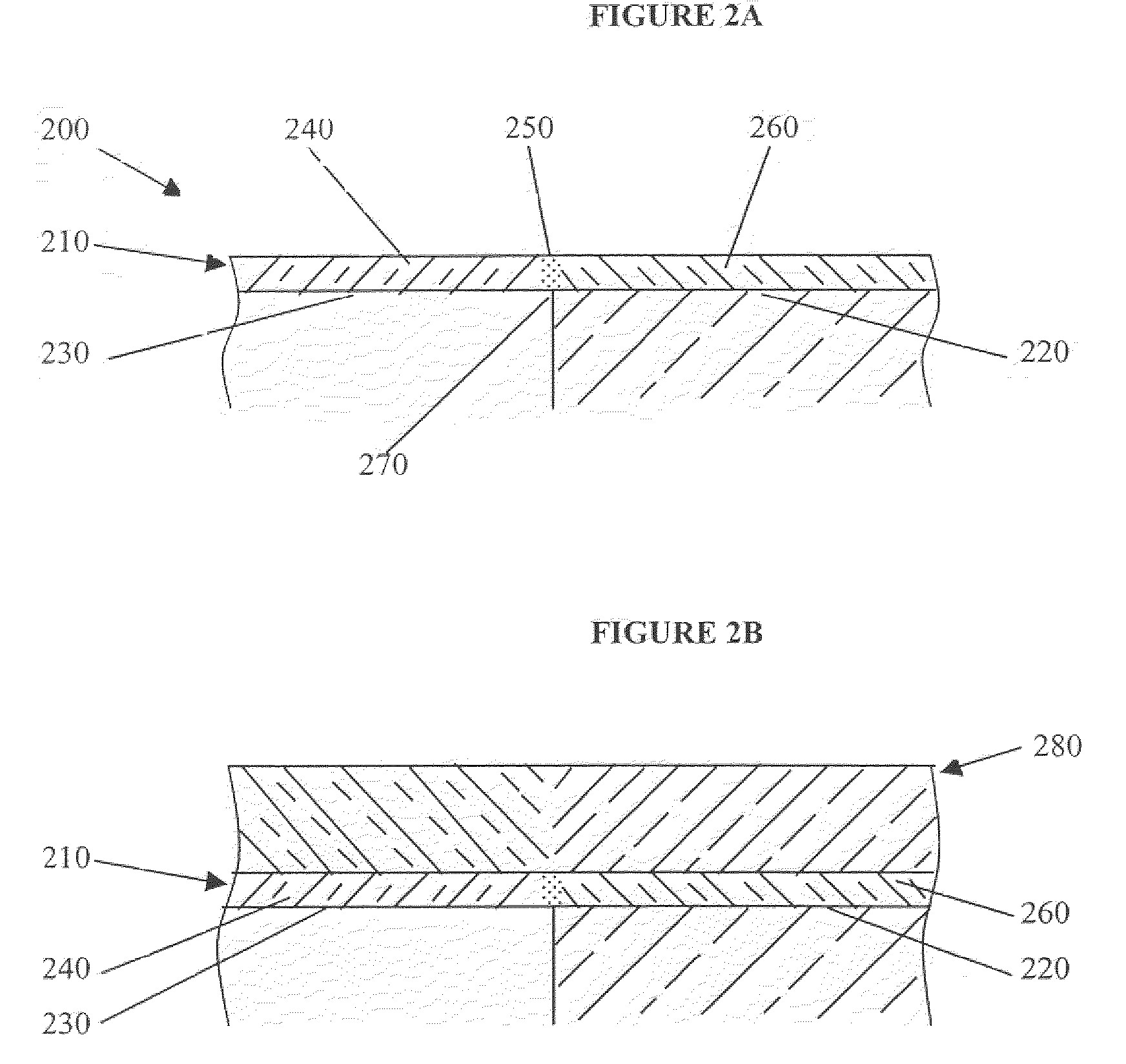
[0013] In another preferred embodiment, a method for reducing the number of steps in a semiconductor device manufacturing process is provided, comprising:identifying a semiconductor device manufacturing process that comprises (a) depositing a first silicon-containing film onto a non-epitaxial surface using a first silicon source and, in a separate step, (b) depositing a second silicon-containing film onto an epitaxial surface using a second silicon source; wherein the first silicon source and the second silicon source are each individually selected from the group consisting of silane, disilane, dichlorosilane, trichlorosilane and silicon tetrachloride; andmodifying the semiconductor device manufacturing process by replacing the first silicon source and the second silicon source with trisilane and simultaneously depositing a third silicon-containing film onto the epitaxial surface and the non-epitaxial surface in the same step.

Problems solved by technology

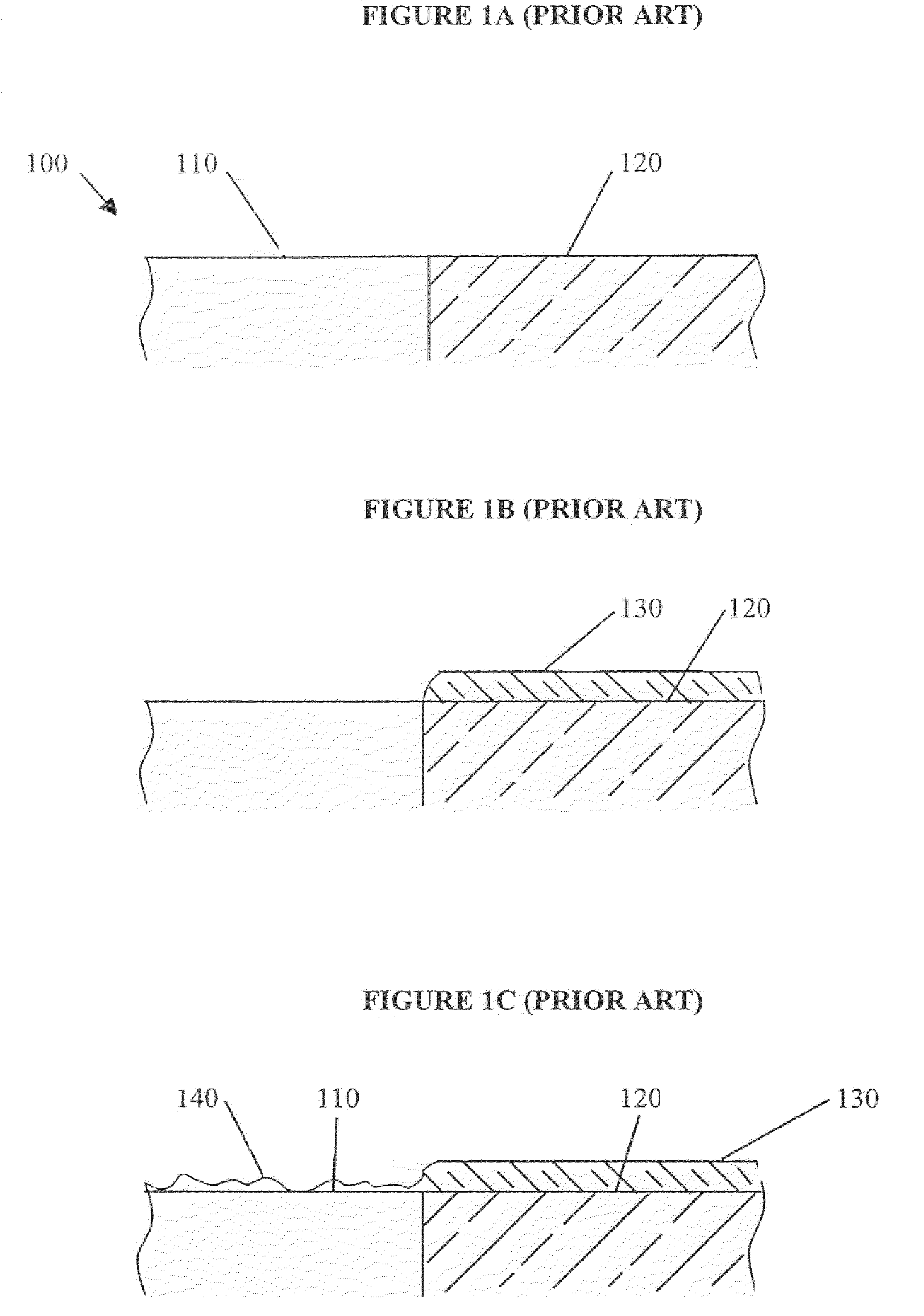
Because of these nucleation issues, deposition of thin film Si-containing materials with similar physical properties onto substrates having two or more different types of surfaces using conventional silicon sources and deposition methods is often problematic.
However, deposition using these conventional silicon sources is generally difficult to control over mixed substrates, such as surfaces containing both single crystal silicon and silicon dioxide.
Control is difficult because the morphology and thickness of the resulting Si-containing film depend on both the deposition temperature and the morphology of the underlying substrate.
Furthermore, deposition tends to be rough over the dielectric since widely spread nucleation sites support deposition while regions between remain bare.
In theory, the deposition parameters could be adjusted to improve the film formation over the oxide surface, but in practice this is rarely an option because such an adjustment would be likely to negatively impact the desired epitaxial film quality.
Therefore, the manufacturer generally has little freedom to adjust the conditions to alter the characteristics of the film over the oxide surface.
Similar problems are also encountered in situations involving other mixed substrates.
In the past, manufacturers have approached such problems through the use of selective deposition or additional masking and / or process steps.
However, additional process steps are generally undesirable because they may increase expense, contamination and / or complication.

Method used


Image

  • Deposition Over Mixed Substrates
  • Deposition Over Mixed Substrates
  • Deposition Over Mixed Substrates

Examples


example 1

[0066] A substrate was provided consisting of a 1500 SiO.sub.2 (oxide) coating deposited onto a Si(100) wafer. The substrate was patterned to remove about 20% of the oxide coating to expose the underlying Si(100) wafer, thus creating a mixed substrate having a single-crystal surface and an amorphous oxide surface. The mixed substrate was then etched in a solution of dilute hydrofluoric acid, rinsed and dried. The mixed substrate was then loaded into an Epsilon E2500.TM.reactor system and subjected to a hydrogen bake at 900.degree.C at atmospheric pressure under a flow of 80 slm of ultra-pure hydrogen for 2 minutes. The mixed substrate was then allowed to reach thermal equilibrium at 600.degree.C at 40 Torr pressure under a flow of 20 slm of ultra-pure hydrogen gas. The steps of etching, drying, rinsing, and baking rendered the single crystal surface active for epitaxial film growth.

[0067] Pure hydrogen gas was then passed through liquid trisilane (maintained at room temperature usin...

example 3

[0072] A Si-containing film was deposited at 600.degree.C as described in Example 2, but trisilane and germane were used in place of silane and germane as precursors. The surface roughness of the resulting SiGe film (as measured by atomic force microscopy) was 18.4 for a 10 micron x 10 micron scan area. SEM of the SiGe film revealed a much more uniform surface, as demonstrated in the SEM micrographs shown in Figures 8 and 9 (same magnifications and tilt angles as Figures 6 and 7, respectively). The relative lack of island-type deposition, as compared to silane, shows that deposition occurred evenly over the surface, and did not proceed by the nucleation and growth mechanism described above in Example 2. This illustrates the relative insensitivity of deposition to surface morphology when trisilane is used, i.e., excellent nucleation of trisilane-deposited layers and consequent smoothness.

examples 4-21

[0073] A series of Si-containing films were deposited onto a SiO.sub.2 substrate (without a nucleation layer) at a pressure of 40 torr using trisilane and germane. The trisilane flow rate was constant at 77 sccm (hydrogen carrier, bubbler) for the examples of Table 1. Germane flow (10% germane, 90% H.sub.2) and deposition temperature were varied as shown in Table 1. Germanium concentration (atomic %) and thickness of the resulting SiGe films were determined by RBS, and surface roughness was determined by atomic force microscopy (AFM). The results shown in Table 1 demonstrate that highly uniform films can be prepared over a range of temperatures and flow rate conditions, particularly over a range of germane concentration, and further illustrate the relative insensitivity of deposition to surface morphology when trisilane is used.

1TABLE 1 Deposition Temp. Germane Thickness Rate Roughness No. (.degree. C.) Flow (sccm) % Ge (.ANG.) (.ANG. / min) (.ANG.) 1 450 25 5.0 34* 8.5 3.2 2 450 50 7...


PUM

PropertyMeasurementUnit
temperatureaaaaaaaaaa
thicknessaaaaaaaaaa
temperaturesaaaaaaaaaa

Abstract

<heading lvl="0">Abstract of Disclosure< / heading> Chemical vapor deposition methods are used to deposit silicon-containing films over mixed substrates. Such methods are useful in semiconductor manufacturing to provide a variety of advantages, including uniform deposition over heterogeneous surfaces, high deposition rates, and higher manufacturing productivity. An example is in forming the base region of a heterojunction bipolar transistor, including simultaneous deposition over both single crystal semiconductor surfaces and amorphous insulating regions.

Description

Cross Reference to Related Applications[0001] This application claims priority to U.S. Provisional Application No. 60 / 268,337, filed February 12, 2001; U.S. Provisional Application No. 60 / 279,256, filed March 27, 2001; U.S. Provisional Application No. 60 / 311,609, filed August 9, 2001; U.S. Provisional Application No. 60 / 323,649, filed September 19, 2001; U.S. Provisional Application No. 60 / 332,696, filed November 13, 2001; U.S. Provisional Application No. 60 / 333,724, filed November 28, 2001; and U.S. Provisional Application No. 60 / 340,454, filed December 7, 2001; all of which are hereby incorporated by reference in their entireties. This application is also related to, and incorporates by reference in their entireties, co-owned and co-pending U.S. Patent Application Serial Numbers: 10 / 074,563; 10 / 074,149; 10 / 074,722; 10 / 074,564; and 10 / 074,534, all of which were filed on February 11, 2002.Background of InventionField of the Invention[0002] This application relates generally to the d...

Claims


Application Information

Patent Timeline
Patent Type & Authority Applications(United States)
IPC IPC(8): C23C16/24C23C16/02C23C16/42C30B25/02H01L21/20H01L21/205H01L21/28H01L21/285H01L21/316H01L21/331H01L21/337H01L21/425H01L21/469H01L21/8238H01L27/092H01L29/51H01L29/737H01L29/78H01L31/18H01L31/20
CPCB82Y10/00Y02E10/547C23C16/0272C23C16/22C23C16/24C23C16/30C23C16/308C23C16/325C23C16/345C23C16/36C23C16/56C30B25/02C30B29/06H01L21/02422H01L21/0243H01L21/0245H01L21/0251H01L21/02529H01L21/02532H01L21/02576H01L21/02579H01L21/02592H01L21/02595H01L21/02598H01L21/0262H01L21/02667H01L21/2257H01L21/28035H01L21/28044H01L21/28194H01L21/28525H01L21/28556H01L21/3185H01L21/32055H01L28/84H01L29/127H01L29/51H01L29/517H01L29/518H01L29/66181H01L29/66242H01L31/1804H01L31/182H01L31/202Y02E10/546Y10S438/933B82Y30/00Y02P70/50H01L21/02271H01L21/02211H01L21/0217
Inventor TODD , MICHAEL A.
Owner ASM IP HLDG BV
Learn More