Wafer level stacked package having via contact in encapsulation portion and manufacturing method thereof

Inactive Publication Date: 2009-01-15
SAMSUNG ELECTRONICS CO LTD
View PDF6 Cites 189 Cited by
  • Summary
  • Abstract
  • Description
  • Claims
  • Application Information

AI Technical Summary

Benefits of technology

[0024]According to example embodiments, a method of manufacturing a wafer level stacked package having a via contact in an encapsulation portion may comprise mounting a plurality of first semiconductor chips on a carrier using an adhesive force such that an active region of the first semiconductor chip faces upward, forming a first encapsulation portion that may have the same height as that of the first semiconductor chip on the carrier, forming a first wiring pattern that may be connected to some of bond pads of the first semiconductor chip, while the first wiring pattern may extend to the first encapsulation portion, mounting a second semiconductor chip that may have a size smaller than that of the first semiconductor chip, while the second semiconductor chip may be connected to the other bond pads of the first semiconductor chip and not connected to the first wiring pattern, forming a second encapsul

Problems solved by technology

However, a semiconductor package using semiconductor chips deposited in a vertical direction may cause difficulty in implementing “fan-out”, i.e., the effective expansion of an interval between neighboring external electrical connections that are connected to narrowly spaced bond pads of a semiconductor.
Problems may occur with such a package, when many wires are used to connect semiconductor chips to connection

Method used


Image

  • Wafer level stacked package having via contact in encapsulation portion and manufacturing method thereof
  • Wafer level stacked package having via contact in encapsulation portion and manufacturing method thereof
  • Wafer level stacked package having via contact in encapsulation portion and manufacturing method thereof

Examples


first example embodiment

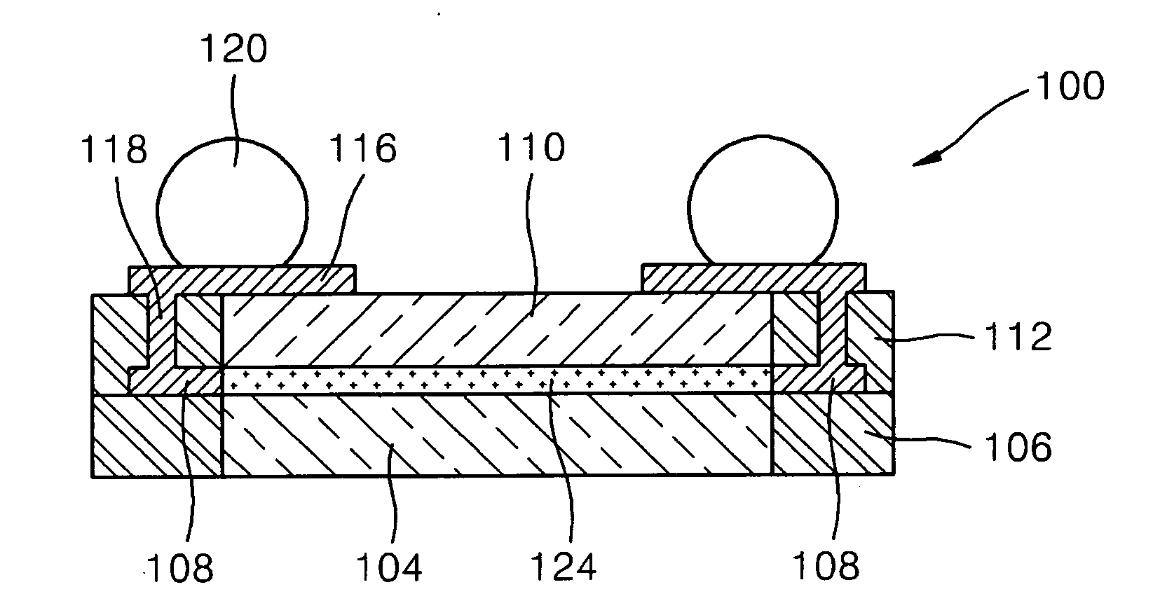
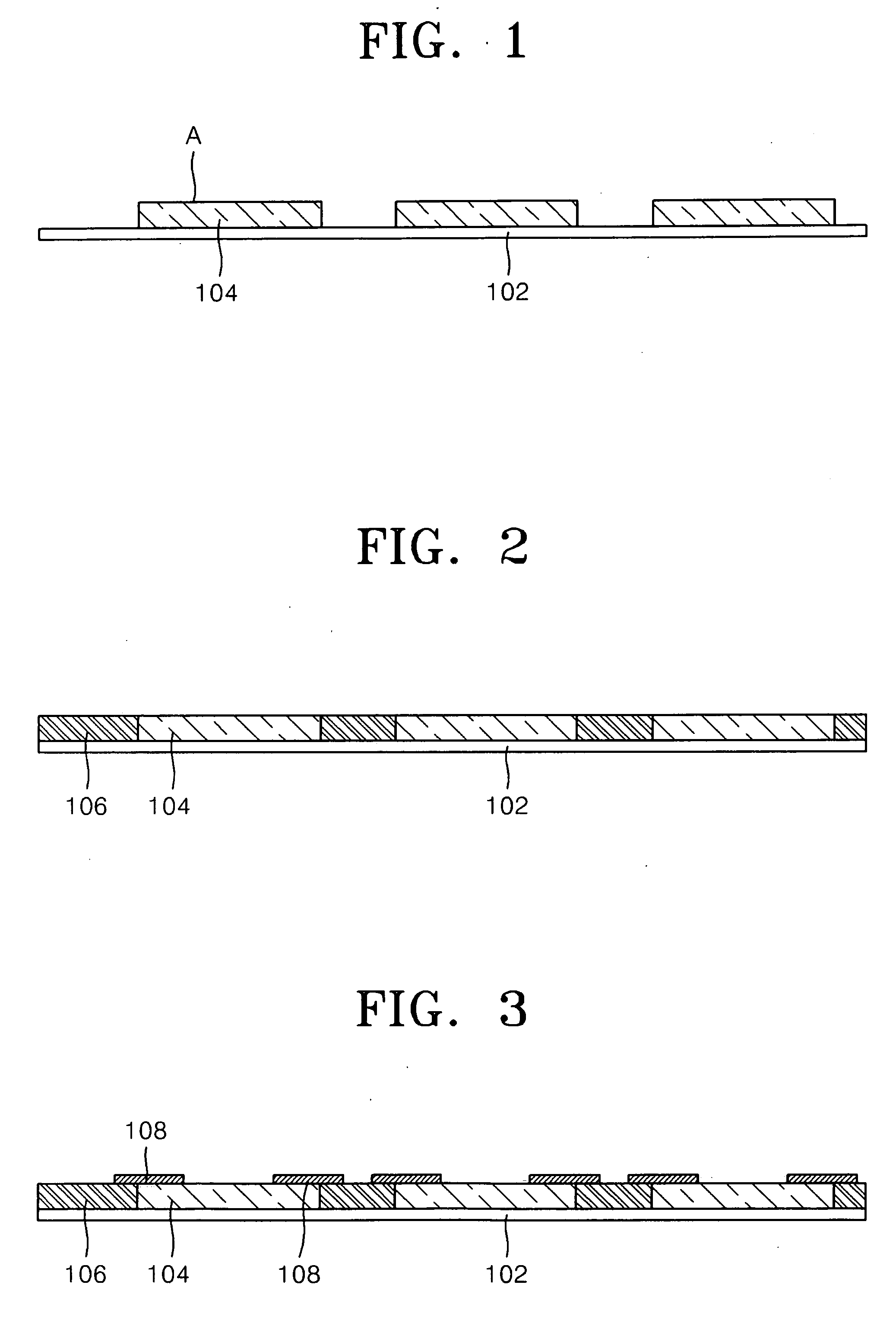
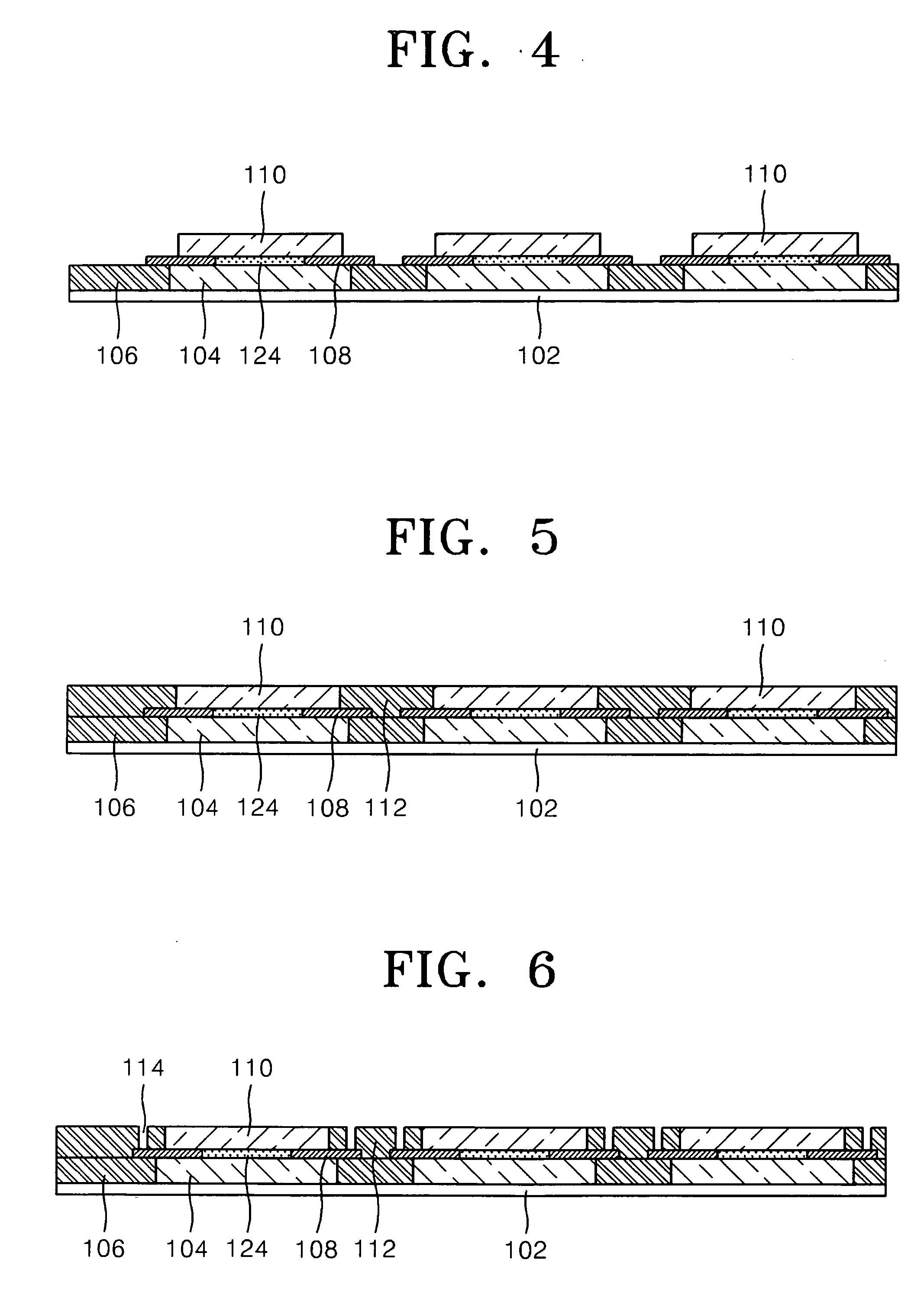
[0043]FIGS. 1 to 9 are cross-sectional views that show a method of manufacturing a wafer level stacked package with a via contact in an encapsulation portion according to example embodiments. Referring to FIG. 1, according to a manufacturing method of a wafer level stacked package according to example embodiments, a plurality of first semiconductor chips 104 may be mounted on a carrier 102 having an adhesive force such that an active region A of each of the first semiconductor chips 104 may face upward. The carrier 102 is preferably a solid substrate where an adhesive layer (not shown) may have an adhesive force that varies according to light or heat, which may be formed on carrier 102.

[0044]Referring to FIG. 2, a first encapsulation portion 106 that may have the same height as that of each of the first semiconductor chips 104 mounted on the carrier 102 may be formed between the first semiconductor chips 104. The first encapsulation portion 106 may be formed in one of the methods se...


PUM


Abstract

Provided are a wafer level stacked package with a via contact in an encapsulation portion, and a manufacturing method thereof. A plurality of semiconductor chips and encapsulation portions may be vertically deposited and electrically connected through a via contact that may be vertically formed in the encapsulation portion. Thus, an effective fan-out structure may be produced, vertical deposition may be available regardless of the type of a semiconductor device, and productivity may be improved.

Description

PRIORITY STATEMENT[0001]This application claims priority under 35 U.S.C. §1.119 to Korean Patent Application No. 10-2007-0070775, filed on Jul. 13, 2007, in the Korean Intellectual Property Office, the entire contents of which are incorporated herein by reference.BACKGROUND[0002]1. Field[0003]Example embodiments relate to a semiconductor package and a manufacturing method thereof, and more particularly, to a wafer level stacked package with a via contact in an encapsulation portion and a manufacturing method thereof.[0004]2. Description of Related Art[0005]Conventionally, the high integration of a semiconductor device has been achieved by either decreasing a line width in a design rule during a wafer manufacturing process or three-dimensionally arranging electronic parts such as a transistor or capacitor to pack a larger number of circuit parts in a limited wafer area. Recently, a method of increasing the integration by mounting a larger number of semiconductor chips in a single sem...

Claims


Application Information

Patent Timeline
IPC IPC(8): H01L23/488H01L21/56
CPCH01L21/6835H01L2224/04105H01L24/18H01L24/82H01L24/96H01L24/97H01L25/0652H01L25/0657H01L25/105H01L2221/68345H01L2224/18H01L2224/76155H01L2224/82039H01L2224/97H01L2225/06513H01L2225/06582H01L2924/01013H01L2924/01029H01L2924/01079H01L2924/15311H01L2924/15331H01L2924/19041H01L23/3185H01L2224/0401H01L2224/82102H01L2224/83H01L2224/12105H01L2924/18162H01L2924/01006H01L2924/01033H01L24/83H01L2225/06565H01L2225/06548H01L2225/1035H01L2225/1058H01L2224/16145H01L2224/32145H01L2224/32245H01L2224/73253H01L2224/73267H01L2224/82H01L2924/3512H01L2924/00H01L2924/181H01L2224/92244H01L21/568H01L24/19H01L2224/82005H01L2224/73209H01L2924/18161H01L23/12
Inventor YOUN, CHEUL-JOONGAHN, EUN-CHULKIM, YOUNG-LYONGLEE, JONG-HO
Owner SAMSUNG ELECTRONICS CO LTD
Why Eureka
Try Eureka