Substrate for mounting semiconductor chips

a semiconductor chip and substrate technology, applied in the direction of electrical apparatus construction details, non-metallic protective coating applications, printed circuit non-printed electric components association, etc., can solve the problems of size and weight, no end to the progress of electronic devices, etc., and achieve the effect of improving connection reliability and high mass productivity

Inactive Publication Date: 2001-08-28
HITACHI CHEM CO LTD
View PDF40 Cites 202 Cited by
  • Summary
  • Abstract
  • Description
  • Claims
  • Application Information

AI Technical Summary

Benefits of technology

The present invention aims at providing a substrate for mounting a semiconductor chip (which may hereinafter be called semiconductor chip mounting substrate) which is improved in connection reliability and also has high mass productivity.

Problems solved by technology

However, there is no end to the progress of electronic devices, and compatibilization of the request for higher performance of electronic devices and the request for reduction in size and weight of circuit-boards is still a serious thesis.

Method used


Image

  • Substrate for mounting semiconductor chips
  • Substrate for mounting semiconductor chips
  • Substrate for mounting semiconductor chips

Examples


example 1

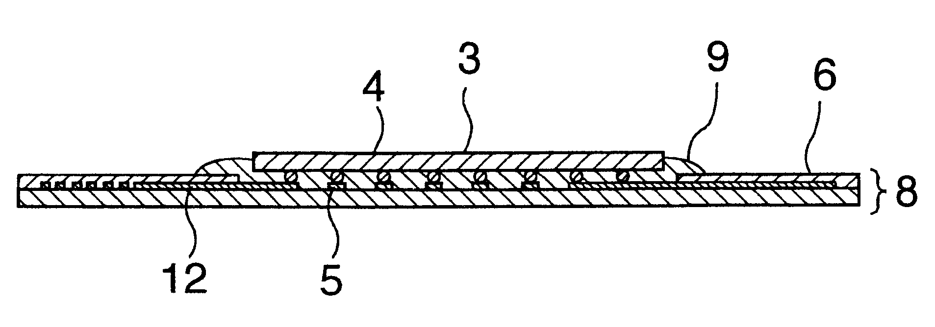
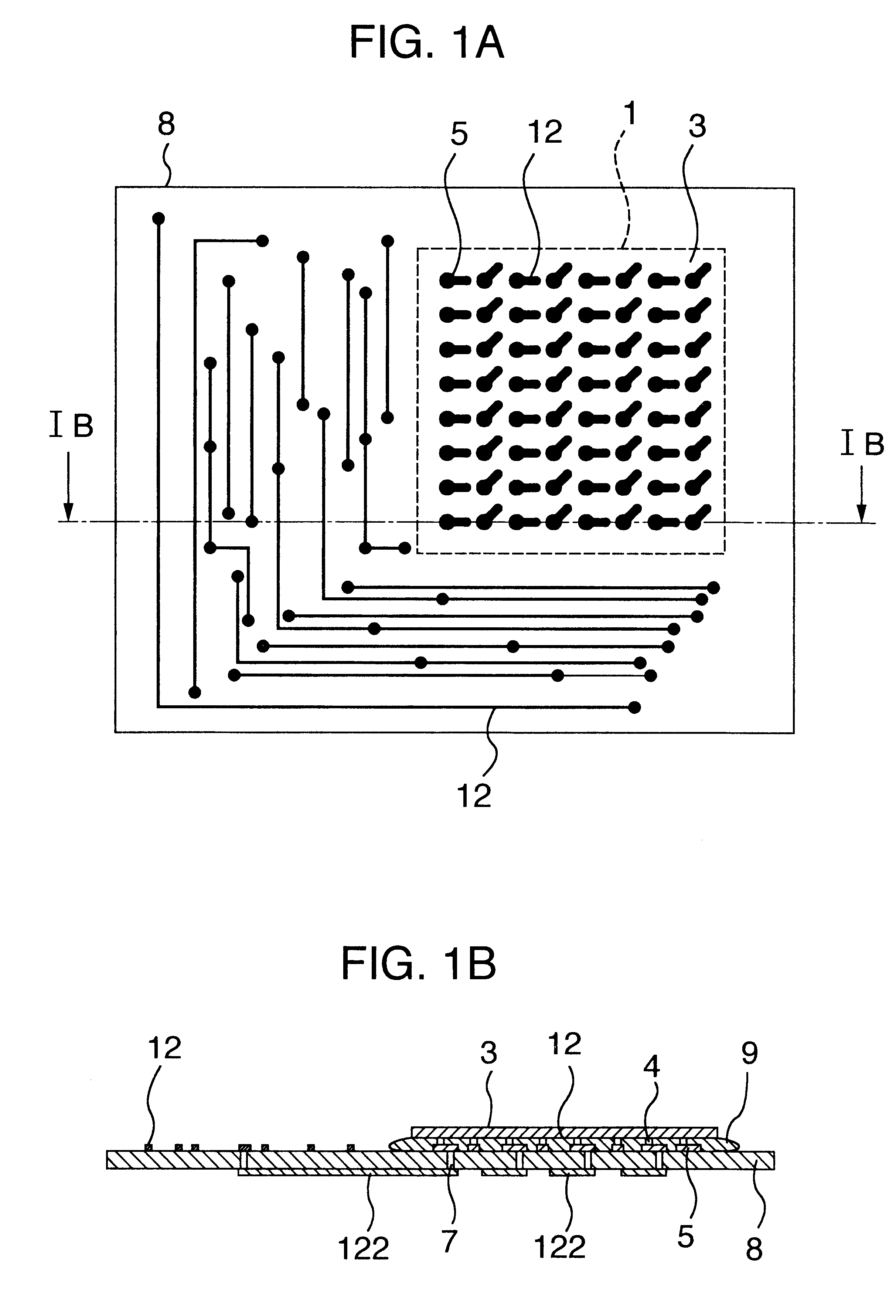
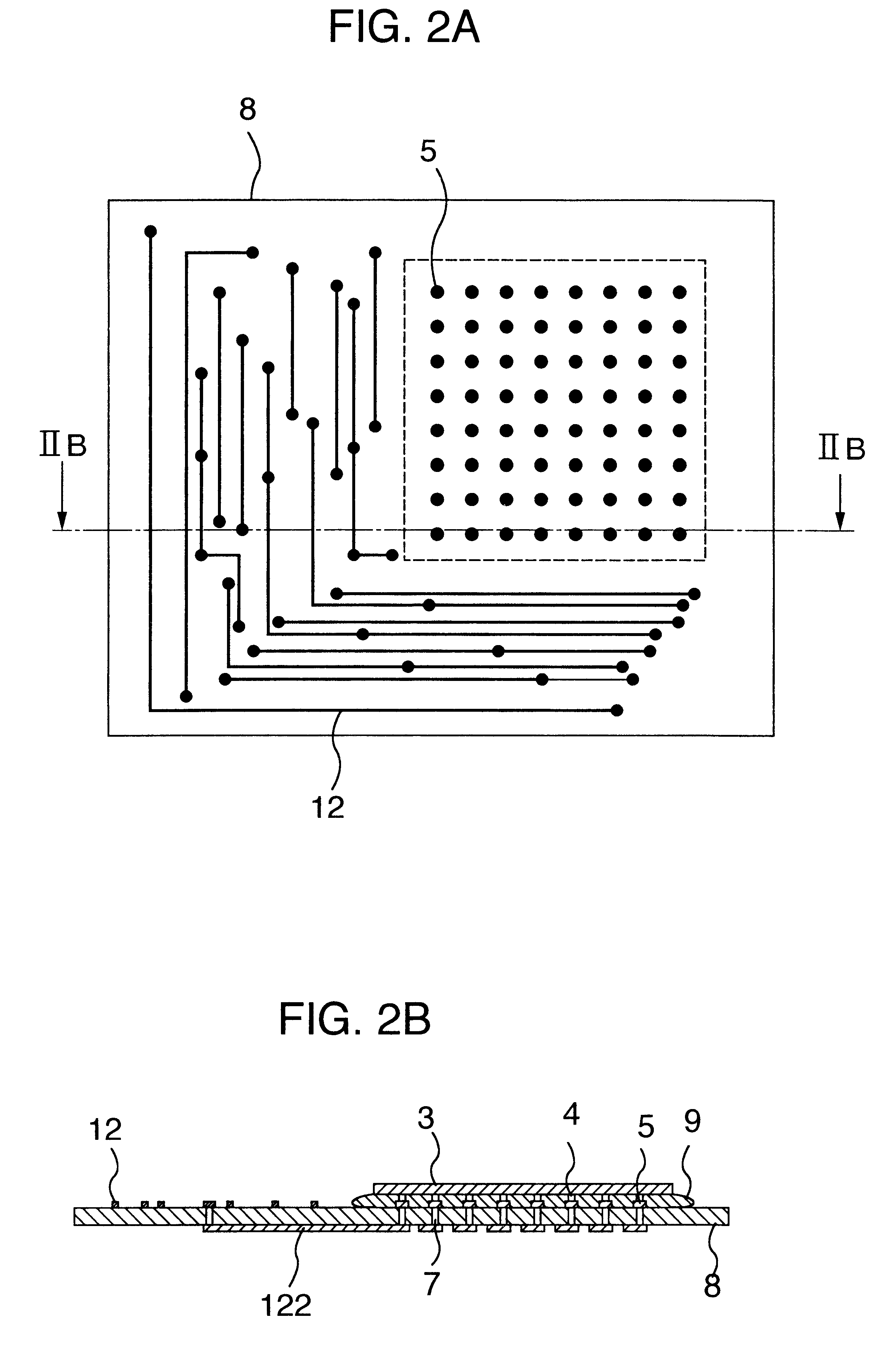
A 0.8 mm thick both-sided copper-clad laminate MCL-E-67 (trade name, produced by Hitachi Chemical Company, Ltd.) having an 18 .mu.m copper foil on both sides thereof, serving as a support in a substrate, was perforated to form the holes that were to become through-holes 7 in FIG. 5B, and immersed in an electroless copper plating solution L-59 (trade name, produced by Hitachi Chemical Company, Ltd.) at 70.degree. C. for 8 hours, causing deposition of 15 .mu.m plating copper. Then unnecessary copper was selectively etched away to form wiring conductors 122, and the through-holes 7 were filled with a resin. The resin used for filling the through-holes 7 was prepared in the following way.

To a 1-liter separable flask equipped with a cocked 25 ml determinate water receiver connected to a reflux condenser, a thermometer and a stirrer, 123.2 g (0.3 mol) of 2,2-bis-[4-(4-aminophenoxy)phenyl]propane, 115.3 g (0.6 mol) of trimellitic anhydride, both as diamines having 3 or more aromatic rings,...

example 2

A semiconductor chip mounting substrate 8 was made in the same way as in Example 1, with the opening 21 of the solder resist 61 being formed smaller than the contour 101 of the semiconductor chip 3.

The ends of the gold wires were melted by a torch or other means to form gold balls, these balls were pressed against an electrode pad, and then the wires were cut out to provide the bumps 4 at the terminal electrodes of the semiconductor chip 3 as shown in FIG. 6B. Further, an anisotropic conductive adhesive Flip Tac (trade name, produced by Hitachi Chemical Company, Ltd.) 91 was disposed between the semiconductor chip mounting substrate 8 and a semiconductor chip 3, and said semiconductor chip 3 was mounted with the upside down on the substrate 8 in registration with the connecting terminals 5 on the substrate and heated and pressed from above under the conditions of 180.degree. C., 30 g / bump and 20 seconds to electrically connect the bumps of the semiconductor chip 3 and the correspond...

example 3

A semiconductor chip mounting substrate 8 was made in the same way as in Example 1, but as shown in FIG. 7A, the wiring conductors 12 on the substrate surface were not formed beneath the contour 1 of the chip, and the opening 21 of the solder resist 61 was formed 100 .mu.m greater than the contour 1 of the semiconductor chip 3.

As shown in FIG. 7B, bumps 4 were formed by plating on the terminal electrodes of the semiconductor chip 3, and further an anisotropic conductive adhesive Flip Tac (trade name, produced by Hitachi Chemical Company, Ltd.) 91 was disposed between the semiconductor chip mounting substrate 8 and a semiconductor chip 3. Said semiconductor chip 3 was mounted with the upside down on the substrate 8 in registration with the connecting terminals on the substrate and heated and pressed from above under the conditions of 180.degree. C., 30 g / bump and 20 seconds to electrically connect the bumps 4 of the semiconductor chip 3 and the semiconductor chip mounting substrate 8...


PUM


Abstract

A substrate for mounting a semiconductor chip having bumps using an adhesive thereon, said substrate being, for instance, provided with an insulating coating having an opening in the semiconductor chip mounting area so that the wiring conductors will not be exposed to the substrate surface near the boundary of the semiconductor chip mounting area, is improved in connection reliability and has high mass productivity.

Description

TECHINICAL FIELDThe present invention relates to a substrate for mounting a semiconductor chip.With advance of electronic devices in recent years, request for reduction in size and weight of the circuit-boards consisting of a wiring board and related electronic arts, not to speak of demand for higher performance of electronic devices, has become more and more intense. Hitherto, the packaging technology has evolved from the system in which DIP or PGA packages were mounted on a wiring board having through-holes to the system in which QFP or BGA packages are mounted on a wiring board having connecting circuits on the surface. Such evolution is credited to the realization of high-density packaging owing to the reduced dead space of the wiring board and facilitation of miniaturization and higher performance of the packages themselves. However, there is no end to the progress of electronic devices, and compatibilization of the request for higher performance of electronic devices and the r...

Claims


Application Information

Patent Timeline
Patent Type & Authority Patents(United States)
IPC IPC(8): H01L21/56H01L23/52H01L23/498H01L21/02H01L23/48H01L23/538H05K3/32H05K3/28H05K1/18H05K1/11
CPCH01L21/563H01L23/49838H01L23/49894H01L23/5386H01L24/32H05K3/323H01L2924/07811H01L2924/01006H01L2224/73204H01L2224/32225H05K2201/10674H01L2224/16225H01L2224/27013H01L2224/73203H01L2224/83051H01L2924/01005H01L2924/01025H01L2924/01027H01L2924/01029H01L2924/01033H01L2924/01046H01L2924/01047H01L2924/01058H01L2924/01074H01L2924/01078H01L2924/01079H01L2924/01082H01L2924/15192H05K1/114H05K1/189H05K3/28H05K2201/09509H01L2924/00012H01L2924/00H01L2924/12042H01L2224/45144H01L2924/00014H01L2224/0401
Inventor URASAKI, NAOYUKISIMADA, YASUSITSURU, YOSHIYUKINAKASO, AKISHIWATANABE, ITSUO
Owner HITACHI CHEM CO LTD
Why Eureka
Try Eureka