Bit line controlling decoder circuit, semiconductor storage device and data reading method thereof
A semiconductor and decoder technology, applied in the field of data readout, which can solve problems such as misreading and leakage current prevention
- Summary
- Abstract
- Description
- Claims
- Application Information
AI Technical Summary
Problems solved by technology
Method used
Image

Examples
Embodiment Construction
[0101] The present invention will be described in detail below based on the embodiments shown in the accompanying drawings.
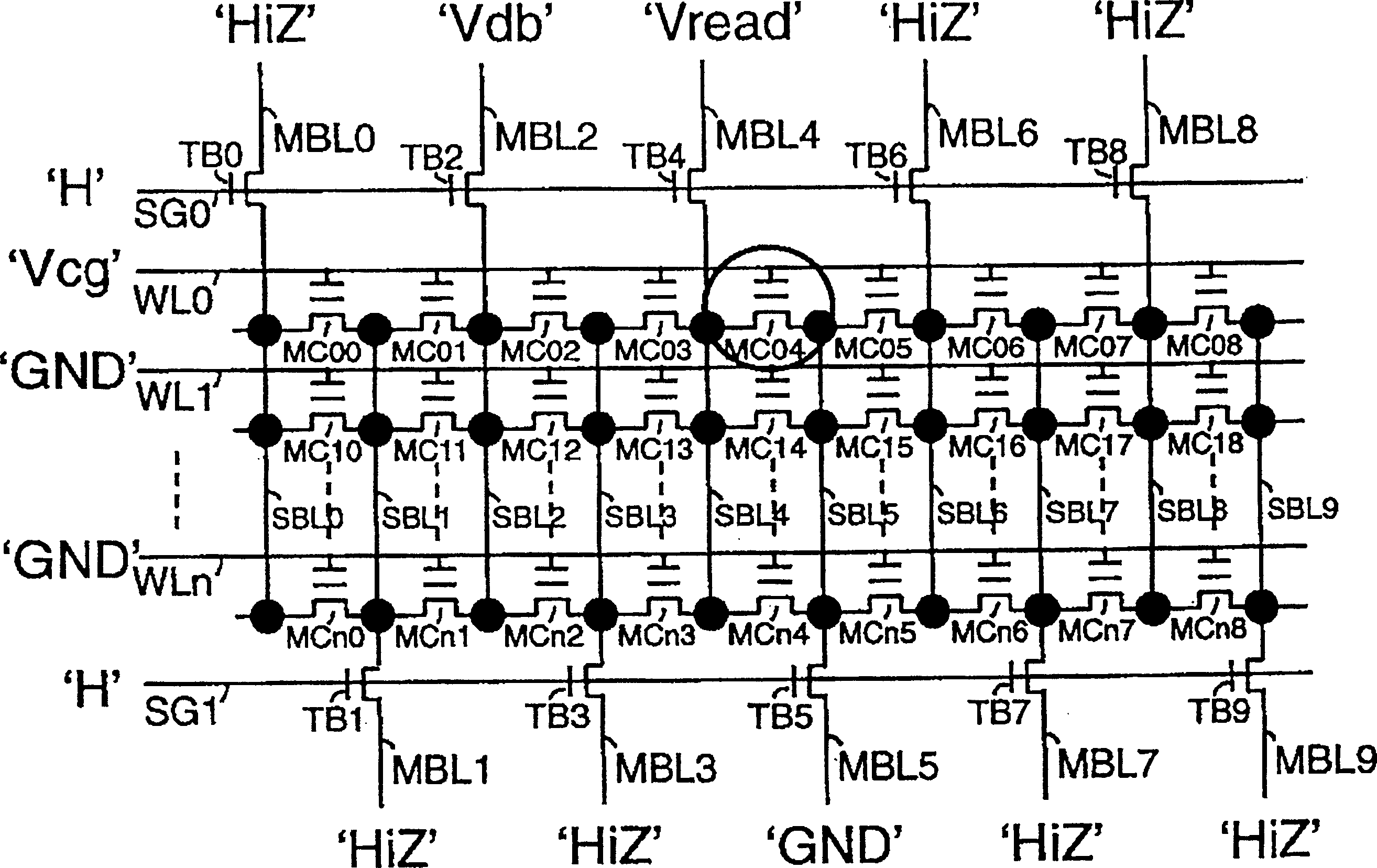
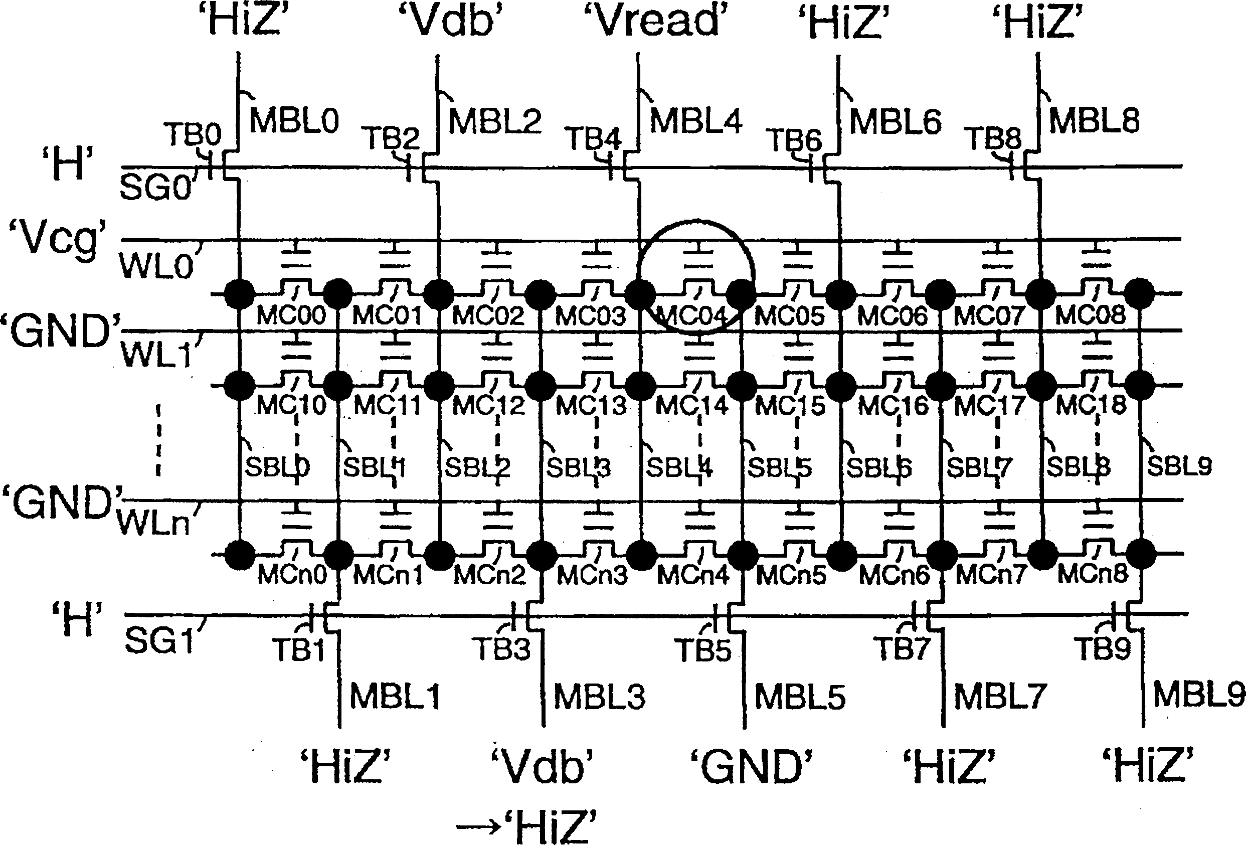
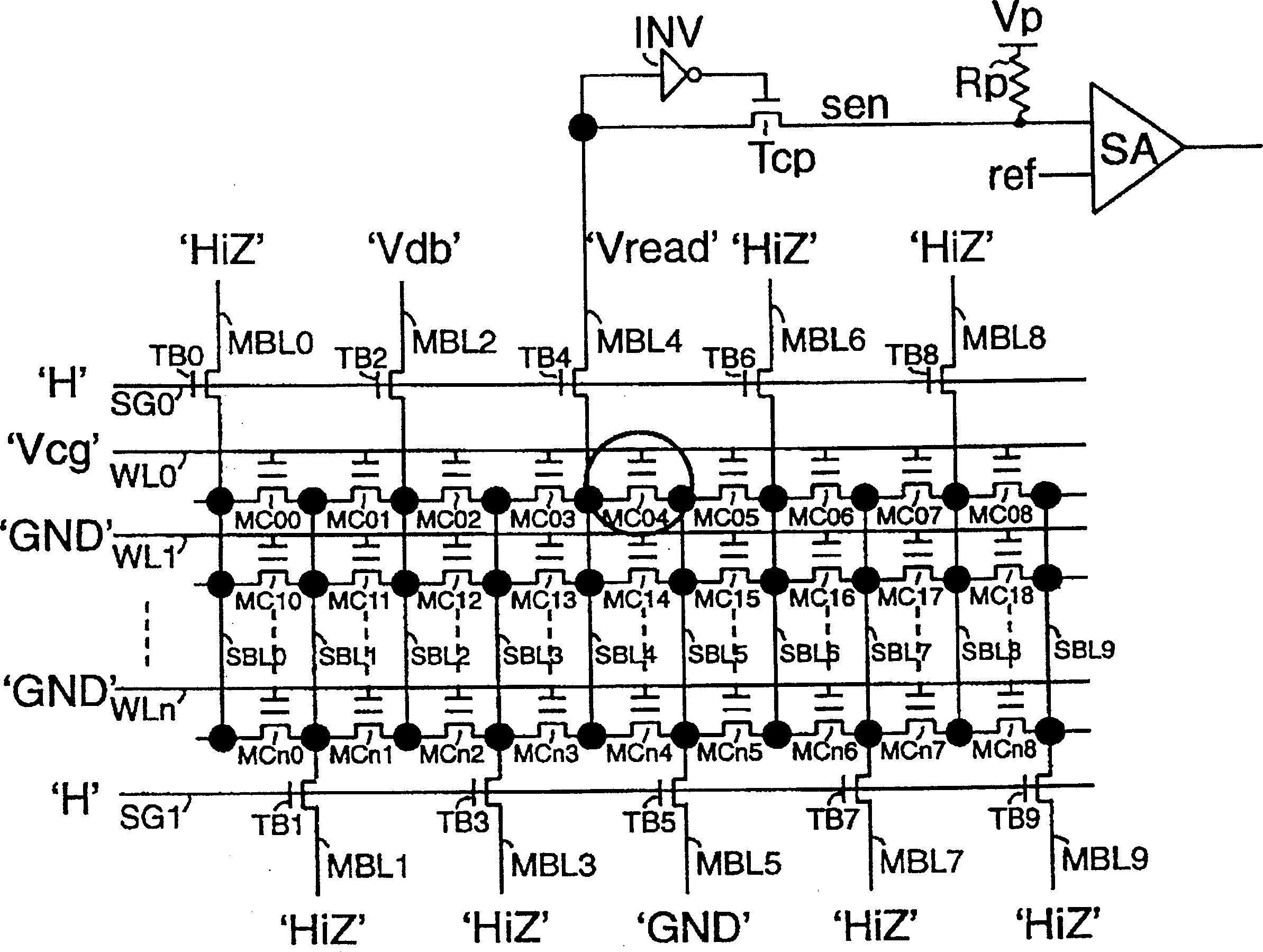
[0102] figure 1 A structure of a memory array of a virtual ground type nonvolatile semiconductor storage device of one embodiment is shown. The memory array is virtually grounded, with one of the blocks of the memory array shown on the diagram. ACT (Asymmetric Contactless Transistor) cells are called memory cells.
[0103]The ACT unit works as follows. It should be noted that FT (Fowler-Nordheim) tunneling is used for writing and erasing. First, read and verify operations will be described. Read and verify operations are performed in the same manner. During readout, such as Figure 9A As shown, a read voltage (verification voltage) is applied to the write line WL of the transistors constituting each memory cell, and a voltage of 1 volt is applied to the source side sub-bit line SB. Then, the sense amplifier performs sense amplification to determ...
PUM
 Abstract
Description
Claims
Application Information
 - R&D
- Intellectual Property
- Life Sciences
- Materials
- Tech Scout
- Unparalleled Data Quality
- Higher Quality Content
- 60% Fewer Hallucinations
Browse by: Latest US Patents, China's latest patents, Technical Efficacy Thesaurus, Application Domain, Technology Topic, Popular Technical Reports.
© 2025 PatSnap. All rights reserved.Legal|Privacy policy|Modern Slavery Act Transparency Statement|Sitemap|About US| Contact US: help@patsnap.com