Supercharge Your Innovation With Domain-Expert AI Agents!

Bit line controlling decoder circuit, semiconductor storage device and data device and data reading method thereof

A semiconductor and bit line technology, applied in the field of data readout, which can solve problems such as misreading and leakage current prevention

Inactive Publication Date: 2003-04-16
SHARP KK
View PDF0 Cites 15 Cited by
  • Summary
  • Abstract
  • Description
  • Claims
  • Application Information

AI Technical Summary

Problems solved by technology

this may cause misinterpretation
Moreover, there is a problem that high-speed readout is prevented by leakage current flowing to adjacent cells even before misread occurs.

Method used


Image

  • Bit line controlling decoder circuit, semiconductor storage device and data device and data reading method thereof
  • Bit line controlling decoder circuit, semiconductor storage device and data device and data reading method thereof
  • Bit line controlling decoder circuit, semiconductor storage device and data device and data reading method thereof

Examples


Embodiment Construction

[0101] Hereinafter, the present invention will be described in detail based on the embodiments shown in the drawings.

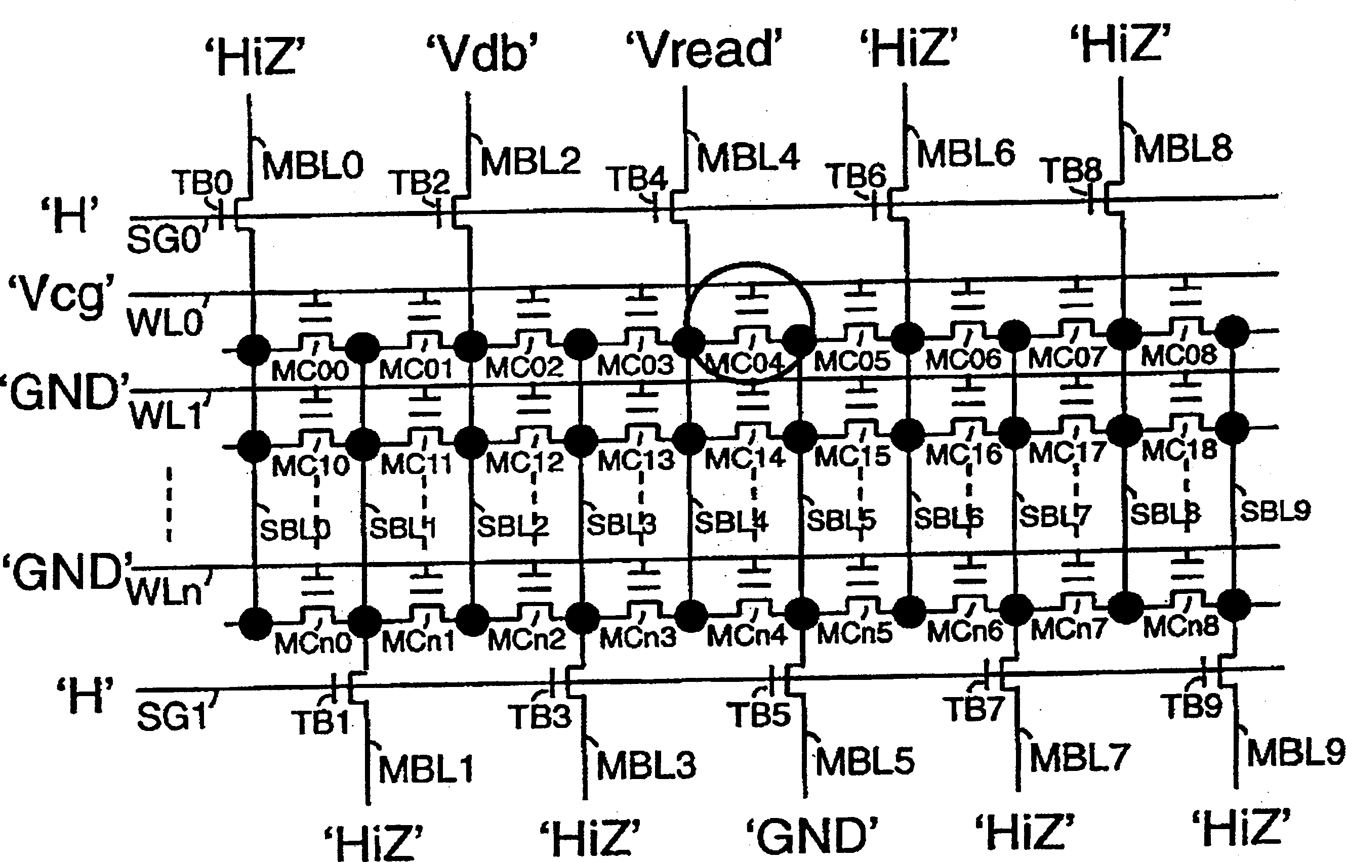
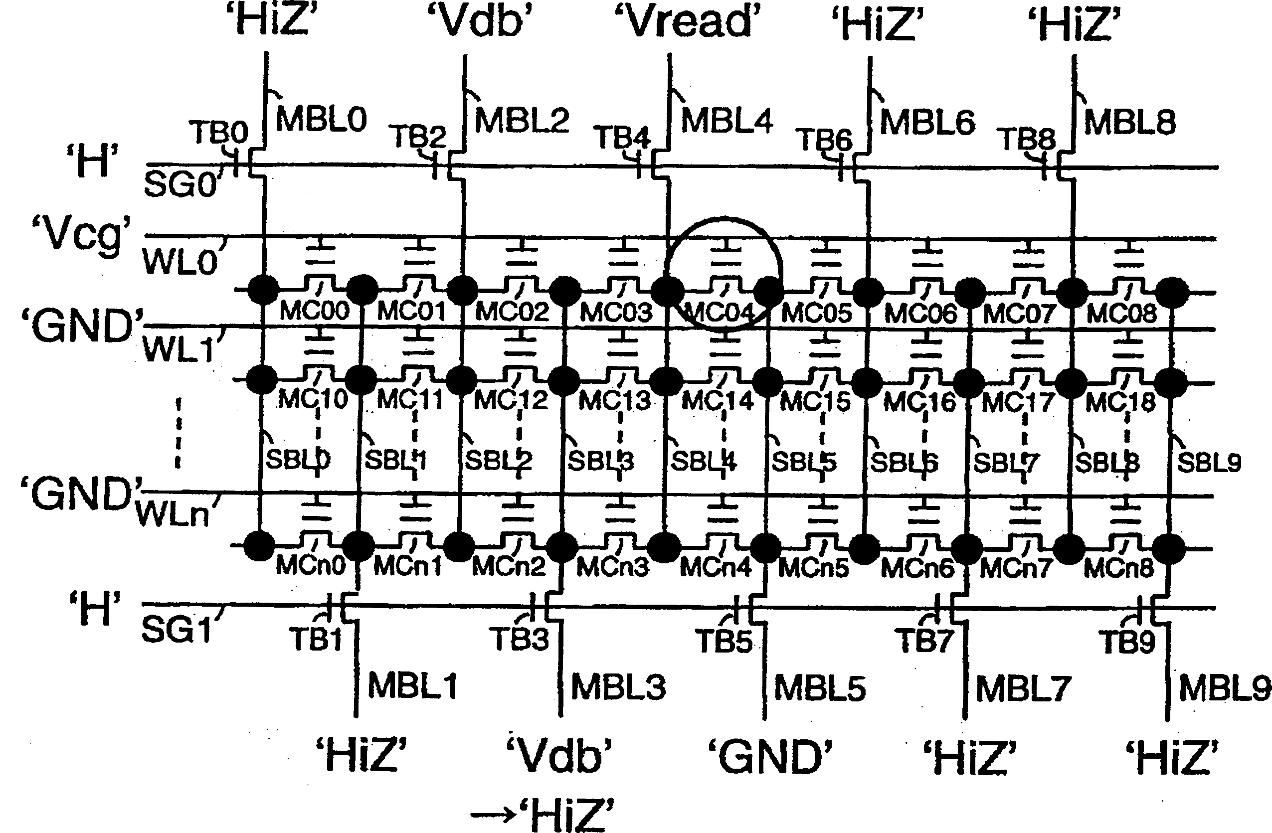
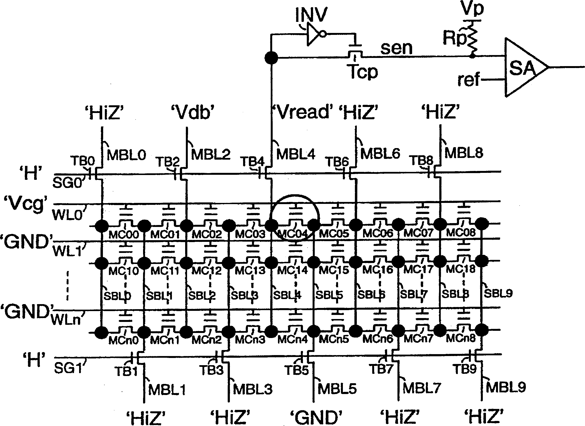
[0102] figure 1 The structure of a memory array of a virtual ground type nonvolatile semiconductor storage device of one embodiment is shown. The memory array is a virtual ground type, and the figure shows one of the blocks of the memory array. ACT (Asymmetric Contactless Transistor) cells are called memory cells.

[0103]The work of the ACT unit is as follows. It should be noted that the FT (Fowler-Nordheim) tunneling effect is used for writing and erasing. First, the read and verify operations will be described. Read and verify operations are performed in the same way. During reading, such as Figure 9A As shown, the read voltage (verification voltage) is applied to the write line WL of the transistor constituting each memory cell, and a voltage of 1 volt is applied to the source side sub-bit line SB. Then, the sense amplifier performs sense amplification to ...


PUM


Abstract

There is provided a virtual ground type nonvolatile semiconductor storage device capable of effectively suppressing a leak current to the adjacent cell and thereby achieving high-speed read. During read operation, a ground potential GND is applied to a bit line SBL5 connected to the source region of one memory cell transistor MC04 subjected to read. Moreover, a read drain bias potential Vread is applied to a bit line SBL4 connected to the drain region of the memory cell transistor MC04. A bit line SBL3 connected to the drain region of a first adjacent memory cell transistor MC03 is put into a floating state. A potential Vdb equal to the read drain bias potential Vread is applied to a bit line SBL2 connected to the drain region of a second adjacent memory cell transistor MC02.

Description

Technical field [0001] The present invention relates to a bit line control decoder circuit, a virtual ground type nonvolatile semiconductor storage device equipped with the decoder circuit, and a data reading method of the virtual ground type nonvolatile semiconductor storage device. Background technique [0002] In recent years, with the development of the functions of portable phones and the expansion of the memory card and file market, the capacity of flash memory is increasing, and devices with small effective cell areas such as multi-value systems and virtual ground array systems have been continuously developed. ) In order to solve the problem of cost reduction. Specifically, the virtual ground array system can achieve a small cell area by designing the circuit it has, thereby allowing devices with a small chip area to be developed through the same processing process. However, because of the virtual ground structure, it cannot be ignored from the memory...

Claims


Application Information

Patent Timeline
IPC IPC(8): G11C16/06G11C11/40G11C16/04G11C16/08G11C16/26
CPCG11C16/26G11C16/0491G11C16/08G11C11/40
Inventor 山本薰伊藤伸彦
Owner SHARP KK
Features
  • R&D
  • Intellectual Property
  • Life Sciences
  • Materials
  • Tech Scout
  • Unparalleled Data Quality
  • Higher Quality Content
  • 60% Fewer Hallucinations
Learn More