Capsulation body of semiconductor ship

A chip packaging and semiconductor technology, applied in semiconductor devices, semiconductor/solid-state device components, electric solid-state devices, etc., can solve the problems of increasing the volume of the semiconductor chip package and increasing the transfer time, so as to improve the signal transfer rate and avoid the signal Distortion, effects that overcome processing limitations

Inactive Publication Date: 2006-02-15
WINBOND ELECTRONICS CORP
View PDF0 Cites 0 Cited by
  • Summary
  • Abstract
  • Description
  • Claims
  • Application Information

AI Technical Summary

Problems solved by technology

However, the first peripheral circuit 35a and the second peripheral circuit 35b will increase the volume of the semiconductor chip package.
In addition, the transfer time of the signal from the first peripheral circuit 35a and the second peripheral circuit 35b in the semiconductor chip to the four regions I, II, III, and IV increases.

Method used


Image

  • Capsulation body of semiconductor ship
  • Capsulation body of semiconductor ship
  • Capsulation body of semiconductor ship

Examples


Embodiment Construction

[0054] In order to make the above-mentioned purposes, features and advantages of the present invention more obvious and understandable, according to the following Figure 3 to Figure 5 Provide preferred embodiments of the present invention, and cooperate with accompanying drawing, describe in detail as follows;

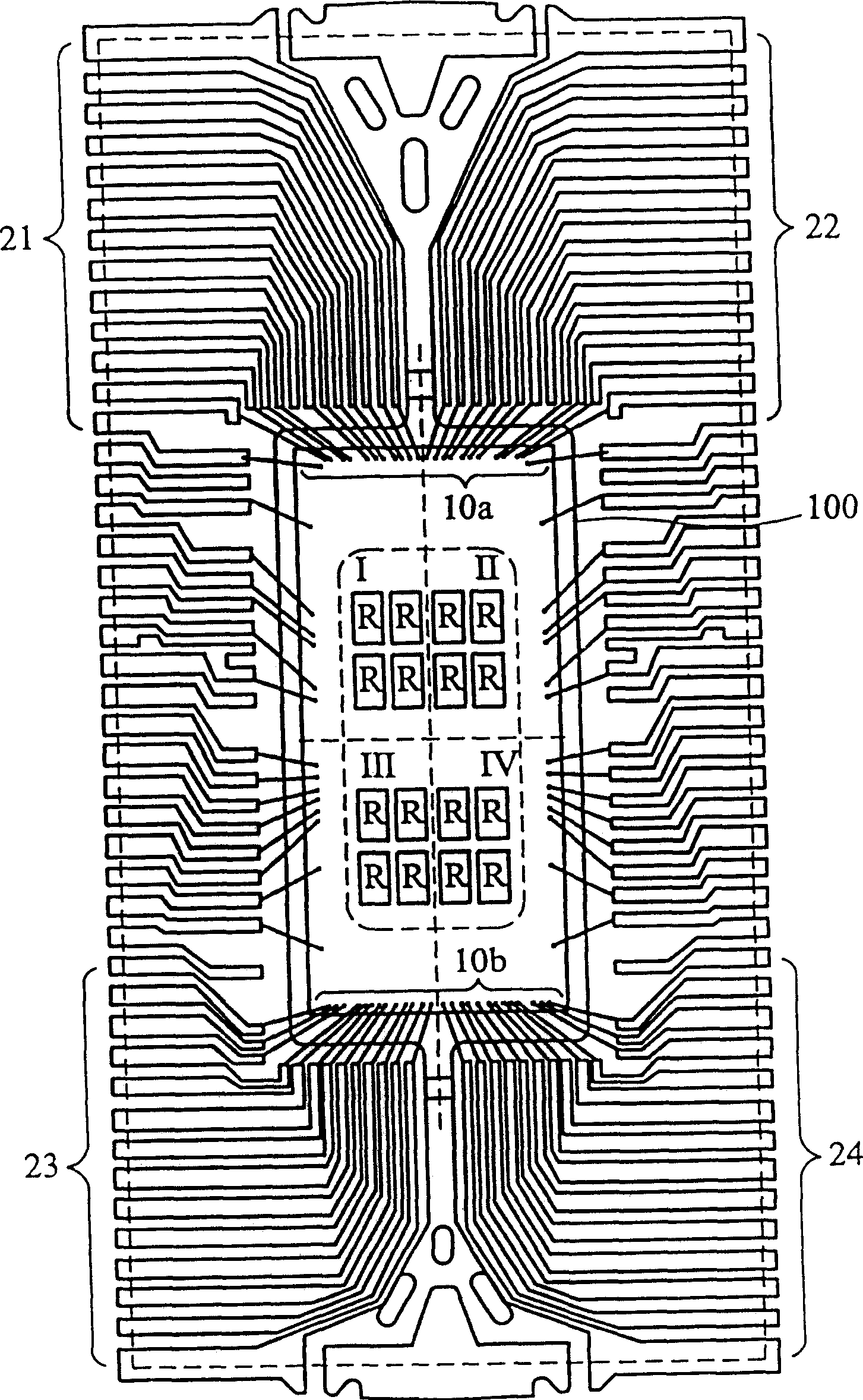
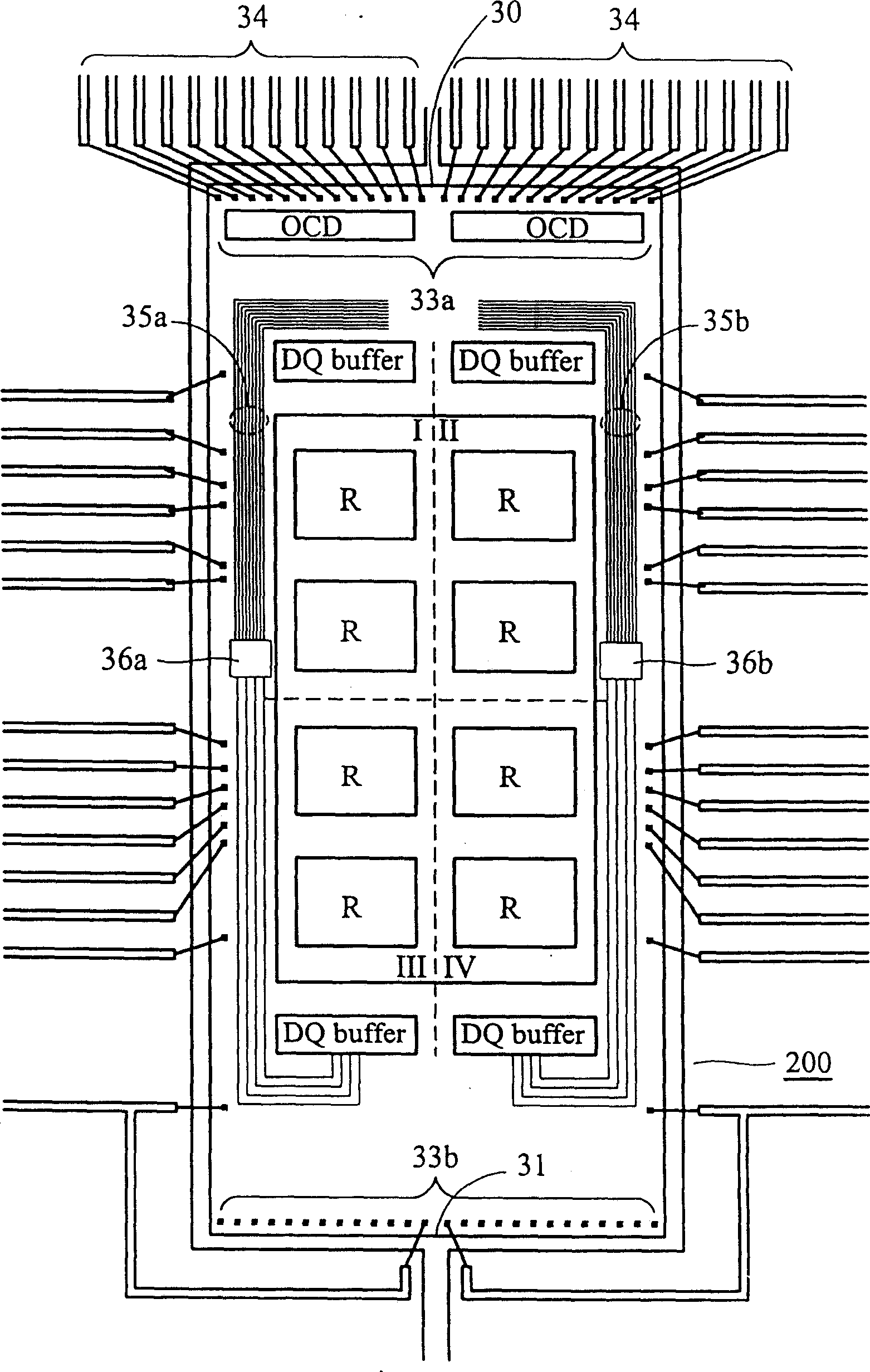
[0055] image 3 It is a plan view showing the semiconductor chip package of the present invention. like image 3 As shown, the semiconductor chip package includes 81 input / output pins, each of which sends and receives different signals.

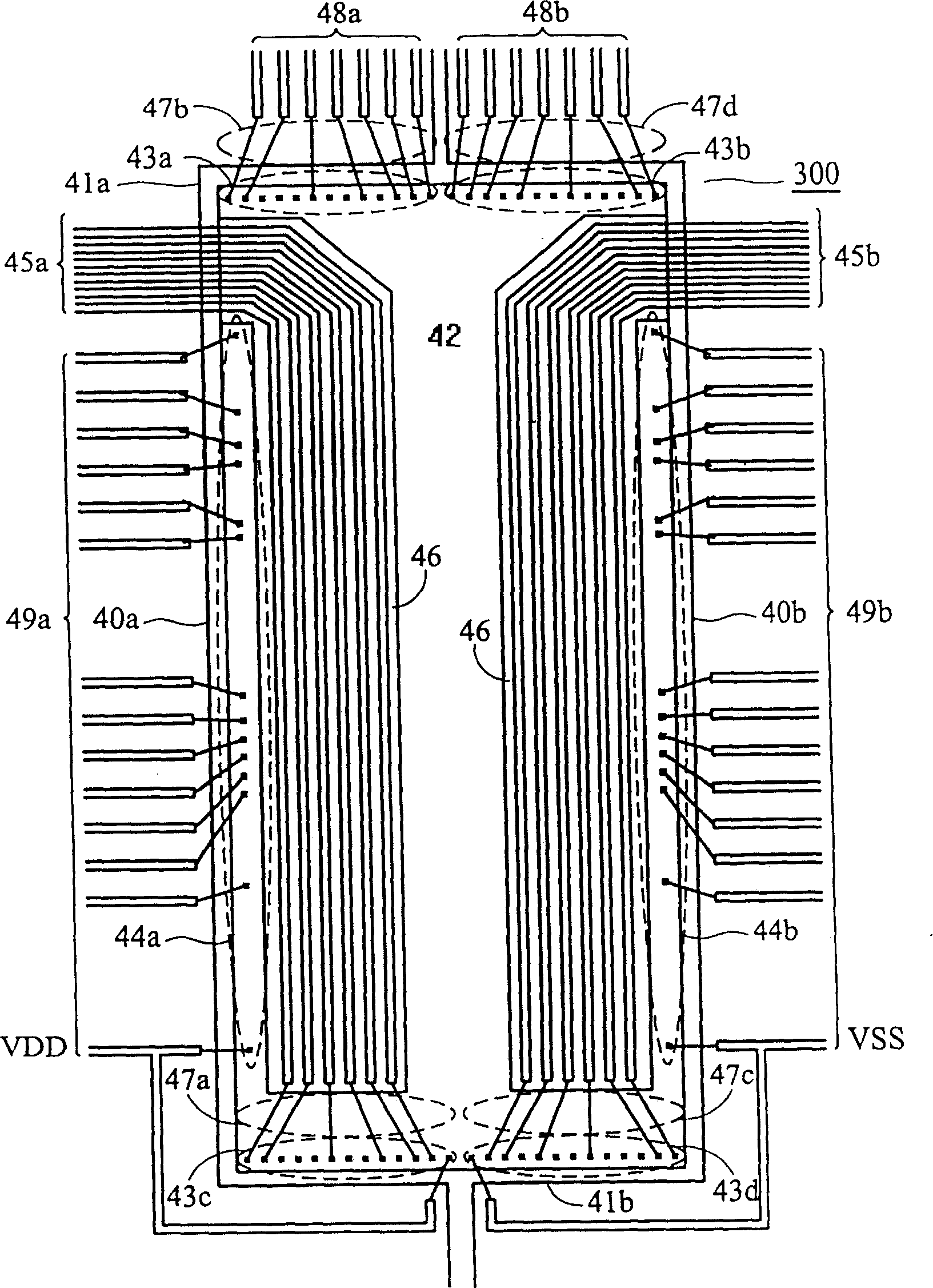
[0056] The semiconductor chip 300 has two long sides 40a and 40b, two short sides 41a and 41b, and an active surface 42 surrounded by the two long sides 40a and 40b. A number of internal circuit components are formed on the active surface 42 of the semiconductor chip 300 , such as random access memory, control gates, metal lines, and a number of peripheral electrode pads. The peripheral electrode pads 43 a , 43 b , 43 c , 43 d , ...


PUM


Abstract

A capsulation body is composed of the semiconductor chip, the lead frame and the packaging body. The chip includes two long edges, two short edges, one active face and several marginal electrode pads. The marginal electrode pads are set along the long edges are the short edges. The lead frame is composed of the several up lead typed lead wires and the standard typed lead wires as well as the outer lead wires. The up lead typed lead wires are connected to the electrode pads on one short edge electrically. The standard typed lead wires are connected to electrode pads on the other short edge and the two long edges electrically. The outer lead lead wires are coupled to the up lead typed lead wires and the standard typed lead wires. The packaging body encapsulates the chip and the lead frame.

Description

technical field [0001] The present invention relates to a semiconductor chip packaging body, in particular to forming integrated circuits of different designs on a semiconductor chip with peripheral electrode pads by using top lead type leads. Background technique [0002] figure 1 It shows a 64Mb semiconductor chip with 32 I / O pins. like figure 1 As shown, on the two short sides of the semiconductor chip 100, there are respectively 24 electrode pads 10a, 10b and standard-type leads 21, 22, 23, 24 connected to the 24 electrode pads. In addition, the semiconductor chip 100 can be divided into four major regions I, II, III, and IV. There are four random access memories R (random access memory) in each area, and eight electrode pads are responsible for data input and output. However, semiconductor crystals of this design have been seldom used. [0003] figure 2 Is to show another 64Mb semiconductor chip with 16 I / O pins. like figure 2 As shown, there are 24 electrode ...

Claims


Application Information

Patent Timeline
Patent Type & Authority Patents(China)
IPC IPC(8): H01L23/48H01L23/50H01L23/28
CPCH01L2224/48247H01L2224/49171
Inventor 林玉漳
Owner WINBOND ELECTRONICS CORP
Why Eureka
Try Eureka