Optical modulator and method for controlling optical modulator

An optical modulator and optical modulation technology, applied in optics, nonlinear optics, instruments, etc., can solve problems such as modulation schemes that cannot be applied to optical duobinary modulation, and achieve reliable detection, compensation of operating point drift, and reduction of chirp sound effect

Inactive Publication Date: 2006-03-29
FUJITSU LTD
View PDF1 Cites 3 Cited by
  • Summary
  • Abstract
  • Description
  • Claims
  • Application Information

AI Technical Summary

Problems solved by technology

Therefore, there arises a problem that the ABC control method employed in the conventional NRZ modulation method cannot be applied to modulation schemes including optical duobinary modulation in which the voltage-optical output characteristic is b

Method used


Image

  • Optical modulator and method for controlling optical modulator
  • Optical modulator and method for controlling optical modulator
  • Optical modulator and method for controlling optical modulator

Examples


no. 1 example

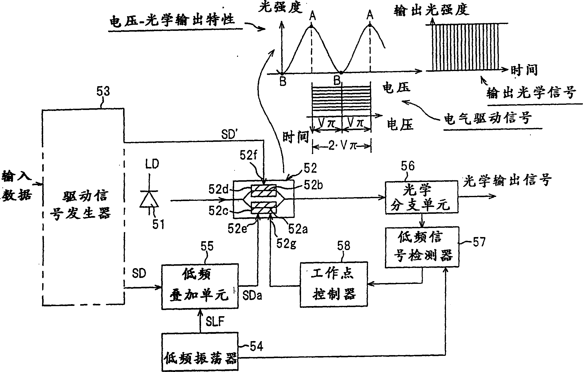
[0124] Figure 7 is a diagram showing the configuration of an optical modulation device according to the first embodiment. This is an example where a LN optical modulator (MZ type optical modulator) configured for two-sided drive (i.e. the modulator has drive electrodes on both sides) is used as the optical modulator, and low frequency is achieved in such a way modulated so that the envelopes on the on and off sides of the modulator voltage drive signal applied to the optical modulator respectively have the same phase (see figure 2 ). Figure 8 With Figure 7 Waveform diagram of the signal concerned.

[0125] expressed in Figure 7 In the center are a semiconductor laser (DFB-LD) 51, and an MZ type optical modulator 52 whose voltage-optical output characteristic changes periodically. The optical modulator 52 includes: some optical waveguides 52a, 52b formed in LiNbO 3 On the substrate, and branched at the light input side and merged at the light output side; two signal ...

no. 2 example

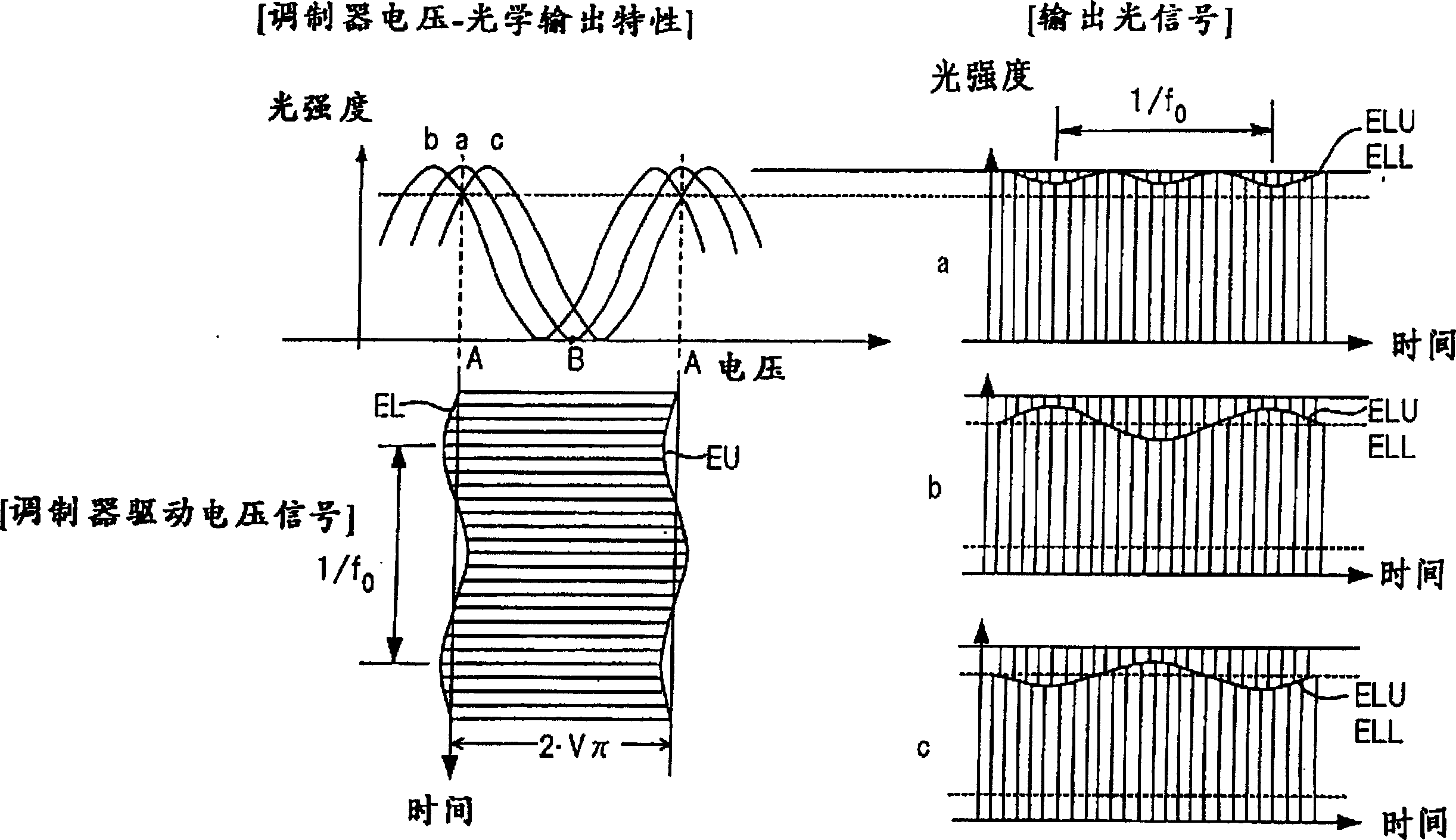
[0149] Figure 13 is a diagram showing the configuration of the optical modulation device according to the second embodiment, and Figure 14 Indicates the relevant signal waveform. The second embodiment differs from the first embodiment in the method of superimposing low-frequency signals. and Figure 7 Elements identical to those shown in are indicated with like reference characters.

[0150] According to the first embodiment, the arrangement is such that the input side of the optical modulator 52 is equipped with a low-frequency superposition unit 55 to change the center voltage of the drive signal SD by a low-frequency signal. However, according to the second embodiment, the gain of the drive circuits 61, 62 is changed by a low frequency signal, whereby the drive signal is amplitude modulated by the low frequency signal.

[0151] expressed in Figure 13 Among them are: semiconductor laser (DFB-LD) 51; MZ type optical modulator 52; driving signal generator 53, which pro...

no. 3 example

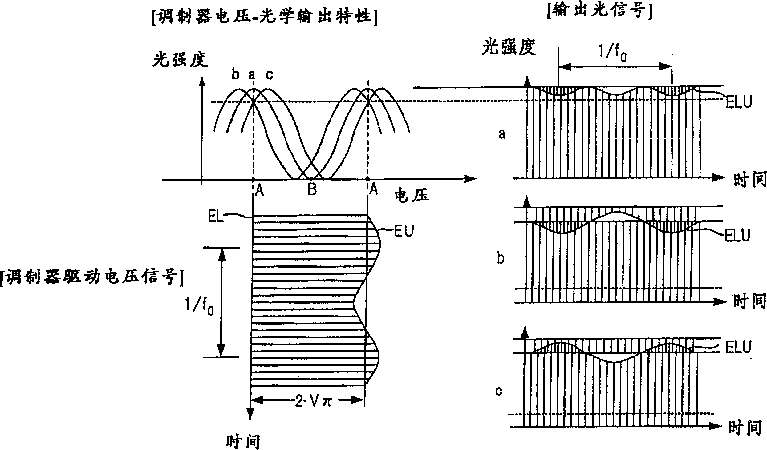
[0163] Figure 17 is a diagram showing the configuration of an optical modulation device according to a third embodiment. and Figure 13 Elements that are the same as those of the second embodiment shown in FIG. 2 are indicated with like reference characters. In a second embodiment, the drive signals SD, SD' are both amplitude modulated by the low frequency signal, whereby the on and off sides of the modulator drive voltage signal are modulated by the low frequency signal having the same phase. In a third implementation, only one of the drive signals SD, SD' is amplitude modulated by the low frequency signal, whereby only the on or off side of the modulator drive voltage signal is modulated by the low frequency signal.

[0164] Figure 17 The third embodiment shown in differs from Figure 13 A second embodiment of the frequency f 0 The low frequency signal SLF is input to the gain control terminal of the driving circuit 61, and is used as the amplitude modulation signal S...


PUM


Abstract

An optical modulator having a voltage-optical output characteristic in which optical output varies periodically with respect to a voltage value of an electrical drive signal is driven by a modulator driving voltage signal, which has an amplitude of 2.Vpi between two light-emission culminations or two light extinction culminations of the voltage-optical output characteristic. A low-frequency superimposing unit superimposes a prescribed low-frequency signal on the modulator driving voltage signal, and an operating-point controller controls the operating point of the optical modulator by detecting operating-point drift of the optical modulator based upon the low-frequency signal component contained in an optical signal output from the optical modulator and controlling the bias voltage of the optical modulator in dependence upon the drift of the operating point of the optical modulator.

Description

technical field [0001] The present invention relates to an optical modulation device and a method of controlling an optical modulator. More specifically, the present invention relates to an optical modulation device and a method of controlling an optical modulator in which even if the operating point of the optical modulator whose optical output varies periodically with respect to a driving voltage, due to ambient temperature or aging Fluctuations can also be compensated for fluctuations in the operating point in a stable manner. More specifically, the present invention relates to a stabilized Mach-Zehnder optical modulator (called MZ type optical modulator) control method of the operating point. Background technique [0002] The amount of available information has increased rapidly in recent years, and there has been a desire to increase the capacity and distance of optical communication systems. In-line optical amplifier systems accommodating 10Gbps transmission speed a...

Claims


Application Information

Patent Timeline
IPC IPC(8): G02F1/01H04B10/14G02F1/03
CPCG02F1/0123G02F2203/21
Inventor 大井宽己中元洋石川丈二山本拓司西泽义德
Owner FUJITSU LTD
Why Eureka
Try Eureka