Transverse electric field liquid crystal display

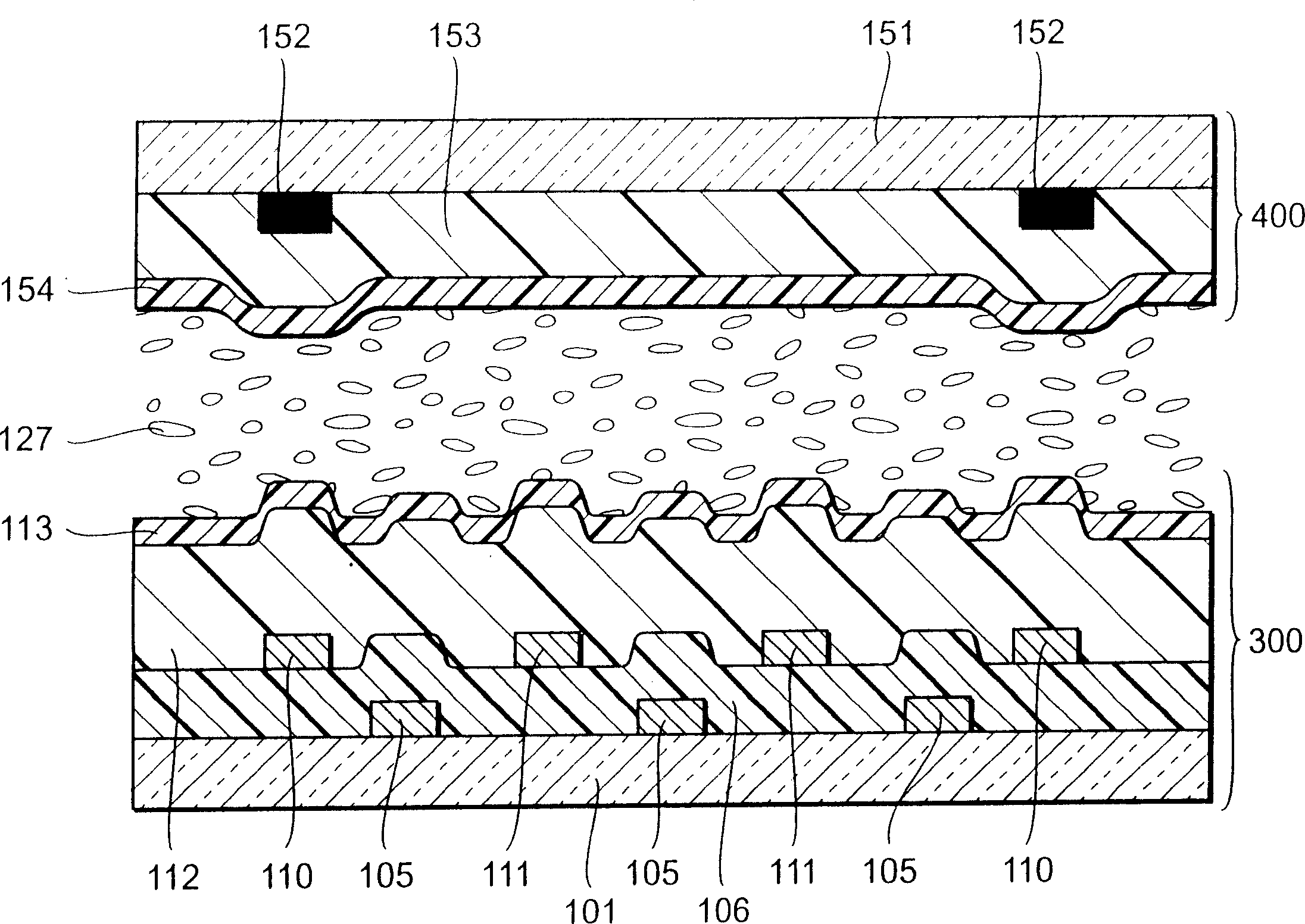
A liquid crystal display, transverse electric field technology, applied in the directions of instruments, circuits, transistors, etc., can solve the problems of uneven friction of the calibration layer 113 and uneven display of the liquid crystal display, etc., to reduce uneven friction, improve smoothness, and uniform friction. Effect

Inactive Publication Date: 2006-04-19
NEC LCD TECH CORP
View PDF0 Cites 0 Cited by
  • Summary
  • Abstract
  • Description
  • Claims
  • Application Information

AI Technical Summary

Problems solved by technology

As a result, the alignment layer 113 becomes uneven due to uneven rubbing, thereby making the liquid crystal display uneven

Method used


Image

  • Transverse electric field liquid crystal display
  • Transverse electric field liquid crystal display
  • Transverse electric field liquid crystal display

Examples


Embodiment Construction

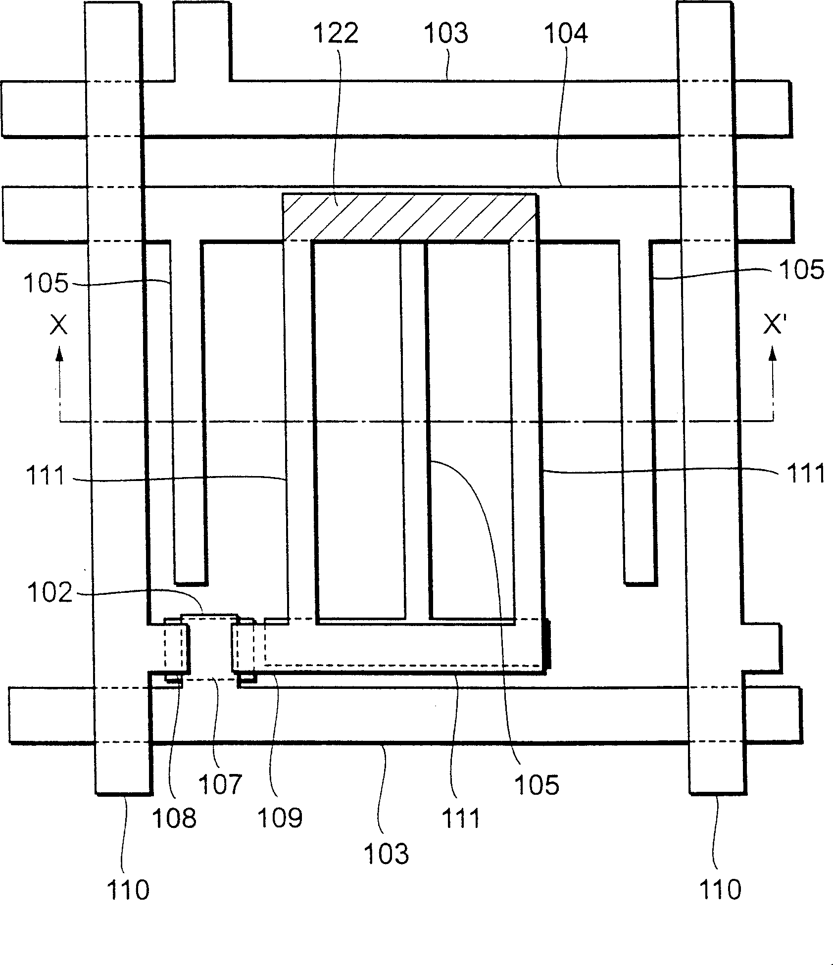
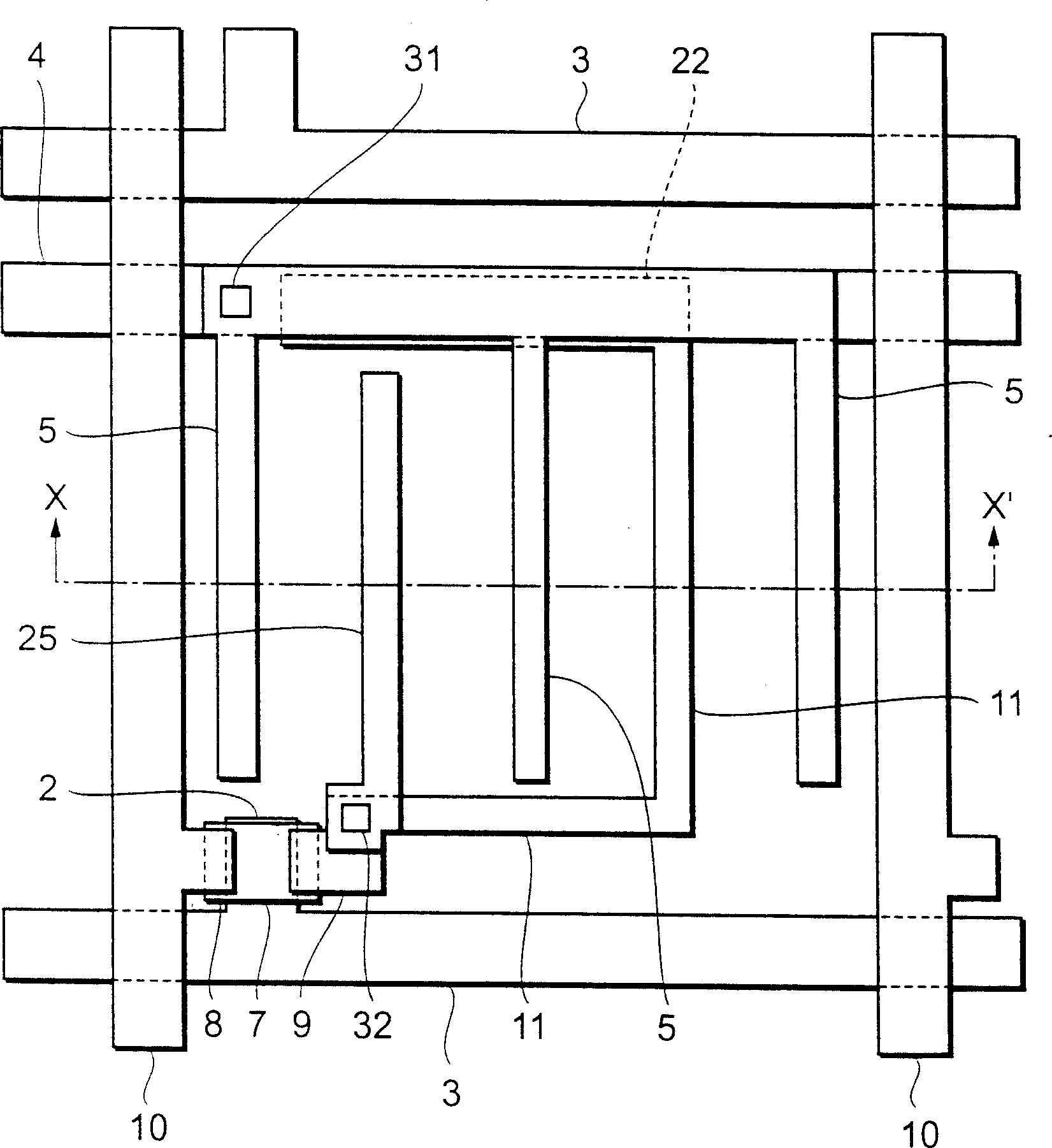
[0020] Hereinafter, examples of liquid crystal displays according to the present invention will be based on image 3 and Figure 4 is described.

[0021] In order to simultaneously form the scanning line 3, the gate electrode 2 connected to the scanning line 3, and the common line 4, a thickness of 200 to 500 nanometers (chromium (Cr), aluminum (Al), or tantalum (Ta), or an alloy of the above metals) A metal film is patterned on a transparent insulating substrate 1 formed of glass, for example. Thereafter, a gate insulating film 6 such as a silicon nitride (SiNx) film having a thickness of 400 to 600 nm is formed over the substrate. Then, a semiconductor island 7 (for example, amorphous silicon or polysilicon) is formed over the gate insulating film 6 . Thereafter, a metal film (chromium, aluminum, or tantalum, or an alloy of the above metals) having a thickness of 200 to 500 nanometers is deposited and patterned to form signal lines 10, source / drain electrodes 8, 9, and co...


PUM

PropertyMeasurementUnit
thicknessaaaaaaaaaa
thicknessaaaaaaaaaa

Abstract

In a lateral electric field liquid crystal display device, a major electrode portion for generating a lateral electric field is formed using a layer different from a layer on which other electrodes and lines are formed. In this case, the major portion is formed to have a thickness of {fraction (1 / 20 to 1 / 3 of the thickness of each of the other electrodes and lines. Thus, flatness of a base film of an alignment layer is significantly improved, also alignment layer material can be coated and formed with high flatness on the base film, and rubbing of the alignment layer material can be performed uniformly for the overall substrate surface.

Description

technical field [0001] The invention relates to a lateral electric field liquid crystal display. The invention specifically relates to an electrode structure of an active element substrate. Background technique [0002] In general, a lateral electric field liquid crystal display is constructed such that a pixel electrode and a common electrode are provided on the same substrate, and an electric field is applied therebetween. Each pixel electrode is connected to an active element, such as a thin film transistor (TFT), to constitute an active matrix substrate (TFT substrate). Liquid crystals are filled between the TFT substrate and the opposite substrate. In such a lateral electric field liquid crystal display, since the liquid crystal is controlled by an electric field acting parallel to the surface of the substrate, a wide viewing angle can be obtained. [0003] The above TFT substrate types will refer to figure 1 and figure 2 to explain. figure 1 It is a view of one ...

Claims


Application Information

Patent Timeline
Patent Type & Authority Patents(China)
IPC IPC(8): G02F1/136G02F1/1345H01L21/3205G02F1/1368G02F1/1333G02F1/1343G09F9/30G09F9/35H01L29/786
CPCG02F1/134363G02F2201/48G02F1/1343
Inventor 浅井卓也黑羽升一佐佐木健
Owner NEC LCD TECH CORP
Why Eureka
Try Eureka