Electric erasing programmable logic element

A technology of programming logic and electrical erasing, applied in electrical components, electrical solid state devices, circuits, etc., can solve the problem of large area of ​​single-layer polysilicon memory cells

Inactive Publication Date: 2006-06-21
EMEMORY TECH INC
View PDF0 Cites 0 Cited by
  • Summary
  • Abstract
  • Description
  • Claims
  • Application Information

AI Technical Summary

Problems solved by technology

[0006] Therefore, the main purpose of the present invention is to provide an electrically erasable programmable logic element, which uses single-layer polysilicon technology, includes a floating gate and a floating ion-doped region, and is used to store data to solve the problem of The above-mentioned problem that the area of ​​the existing single-layer polysilicon storage unit is too large

Method used


Image

  • Electric erasing programmable logic element
  • Electric erasing programmable logic element
  • Electric erasing programmable logic element

Examples


Embodiment Construction

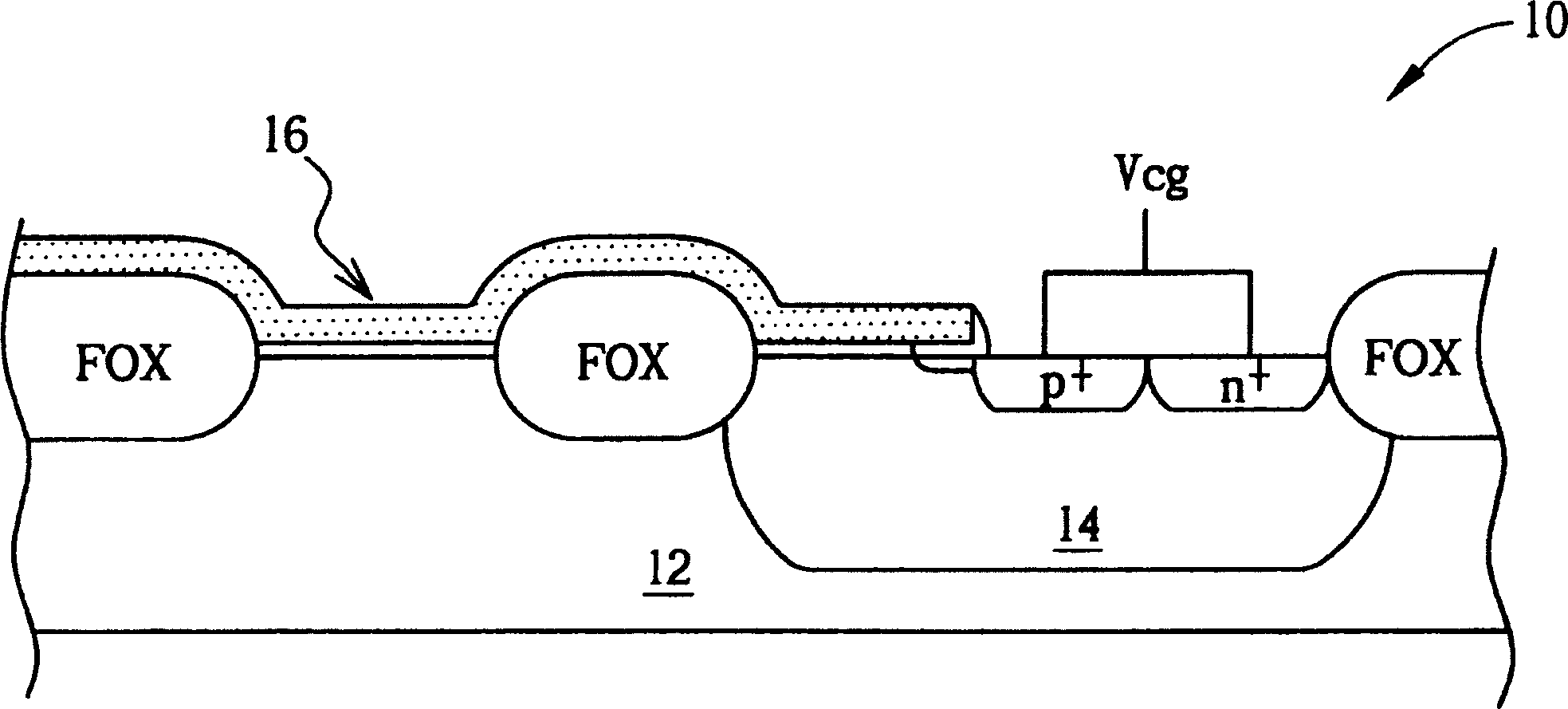
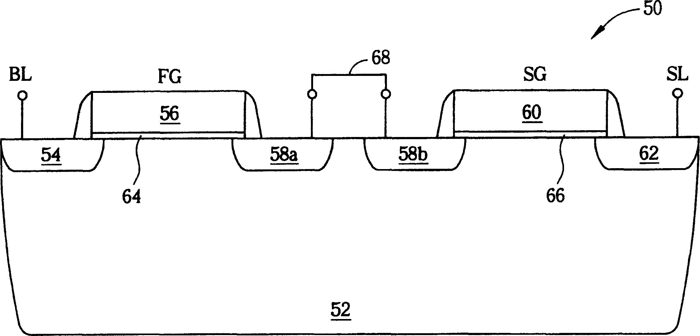
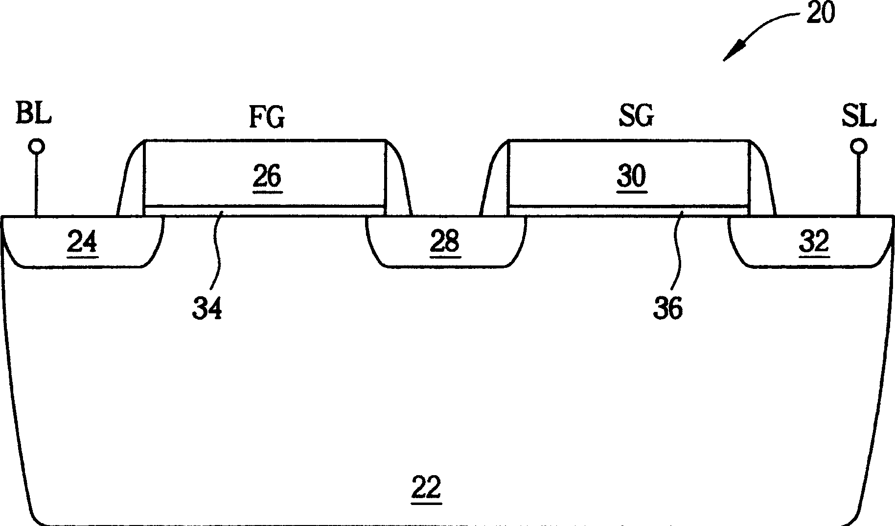
[0034] see figure 2 , figure 2 A front sectional view of an Electrically Erasable Programmable Logic Device (Electrically Erasable Programmable Logic Device) 50 of the present invention is shown in FIG. The electrically erasable programmable logic element 50 includes a P-type substrate (P-Type Substrate) 52; a first N-type ion-doped region 54, located in the P-type substrate 52; a first gate 56, which Located above the P-type substrate 52 and adjacent to the first N-type ion-doped region 54, and in a floating (Floating) state, used as a floating gate of the electrically erasable programmable logic element 50 to store The nonvolatile data of the electrically erasable programmable logic element 50; a second N-type ion-doped region 58a, located in the P-type substrate 52 and adjacent to the first gate 56; a third N-type The ion-doped region 58b is located in the P-type substrate 52 and is electrically connected to the second N-type ion-doped region 58b; a second gate 60, whic...


PUM


Abstract

The invention discloses an electrically erasable programmable logic element, which comprises a P-type substrate; a first N-type ion-doped region located in the P-type substrate; a first gate located in the P-type substrate. On the P-type substrate and adjacent to the first N-type ion-doped region, and in a floating state, used to store data; a second N-type ion-doped region, located in the P-type substrate and connected to the P-type substrate The first gate is adjacent; a second gate, as a control gate, is located on the P-type substrate and is adjacent to the second N-type ion-doped region; a third N-type ion-doped region region, located in the P-type substrate and adjacent to the second gate.

Description

technical field [0001] The invention relates to an electrically erasable programmable logic element, in particular to an electrically erasable programmable logic element which can be manufactured by using a standard CMOS process, and does not require additional floating gate area to reduce volume. Background technique [0002] In recent years, as the demand for portable electronic products increases, the technology and market application of Electrically Erasable Programmable Read-Only Memory (hereinafter referred to as EEPROM) are becoming increasingly mature and expanding. The fields of application of EEPROM include products such as digital camera negatives, mobile phones, video game consoles (Video Game Console), personal digital assistant (Personal Digital Assistant, PDA) memory cards, telephone answering devices, and programmable ICs. EEPROM is a kind of non-volatile memory (Non-Volatile Memory). Its operating principle is to control the opening or closing of the corresp...

Claims


Application Information

Patent Timeline
Patent Type & Authority Patents(China)
IPC IPC(8): H01L27/115
Inventor 李昆鸿徐清祥金雅琴沈士杰何明洲
Owner EMEMORY TECH INC
Why Eureka
Try Eureka