Liquid crystal display with double-film transister pixel structure

A liquid crystal display, switching transistor technology, applied in the direction of transistors, instruments, optics, etc., can solve the problems of short charging time, line ripple, changes, etc., to achieve high display frequency, high resolution, and reduce the effect of feed-through voltage

Inactive Publication Date: 2006-12-06
AU OPTRONICS CORP
View PDF0 Cites 0 Cited by
  • Summary
  • Abstract
  • Description
  • Claims
  • Application Information

AI Technical Summary

Problems solved by technology

Therefore, when the ratio of the channel width to the channel length of the thin film transistor 60 is increased, the capacitance value of the gate-drain capacitance is also increased, resulting in V FD value change
Especially when making a large-sized liquid crystal display, because the panel is too large, the current manufacturing process mostly divides the panel into several areas and exposes them in batches. There will be different offsets, coupled with the effect of increasing the ratio of channel width to channel length, it is quite easy to produce stitching defects, which makes the final liquid crystal display produce the phenomenon of shot mura, which becomes a process An insurmountable obstacle
[0012] Therefore, how to develop a liquid crystal display with high resolution and high display frequency can not only solve the problem of too short charging time, but also avoid line ripples ( shot mura) phenomenon has become a very important issue

Method used


Image

  • Liquid crystal display with double-film transister pixel structure
  • Liquid crystal display with double-film transister pixel structure
  • Liquid crystal display with double-film transister pixel structure

Examples


Embodiment Construction

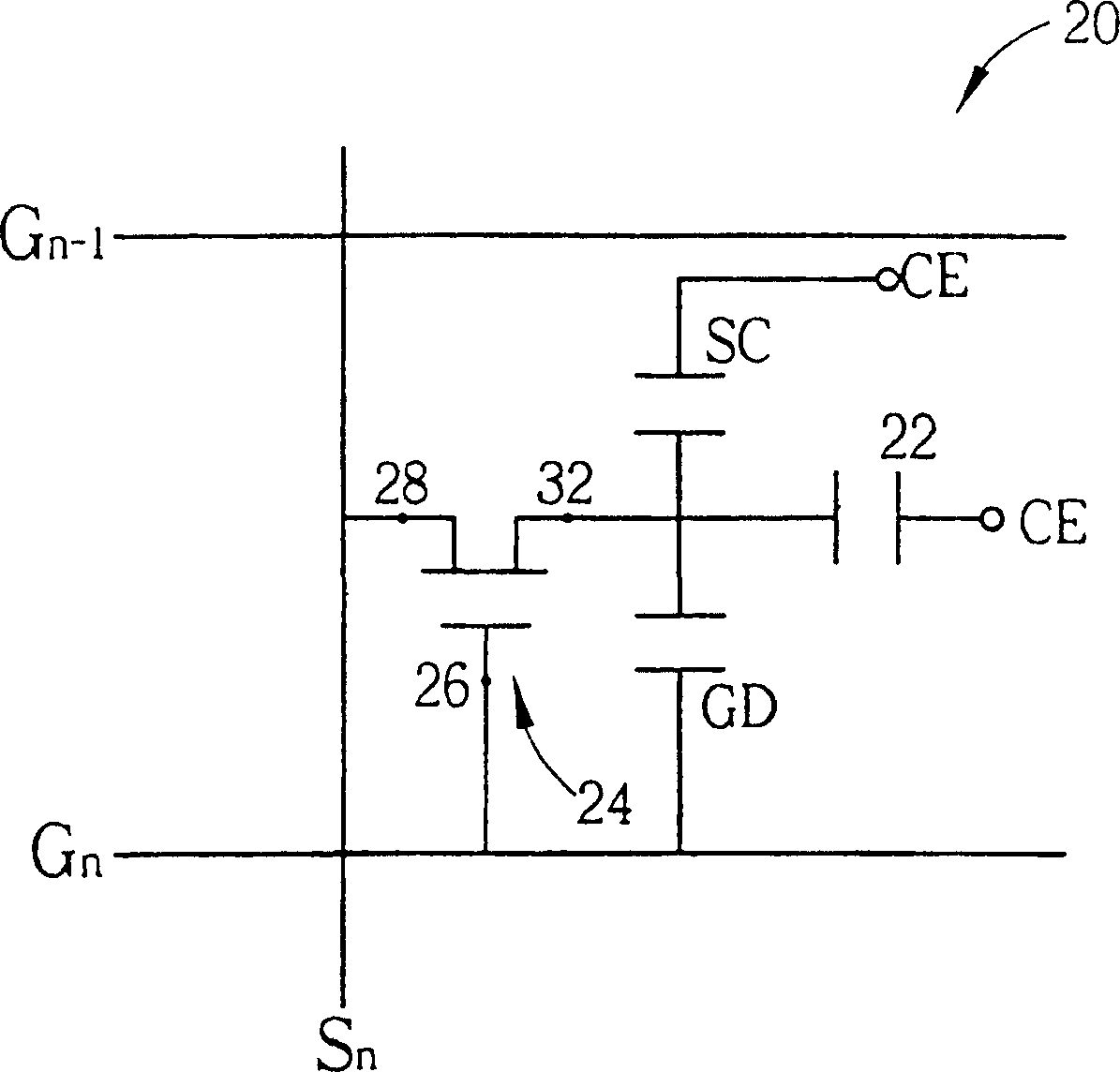
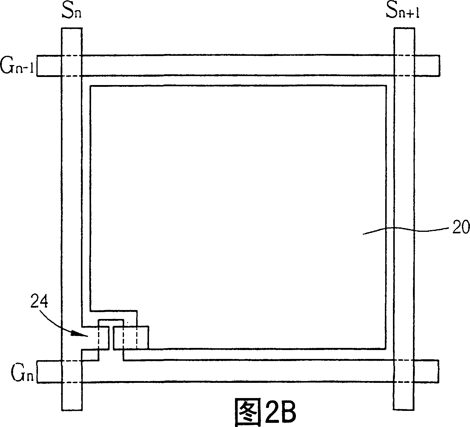
[0024] Please refer to Figure 5, Figure 5A is a schematic diagram of an equivalent circuit of each pixel 100 of the present invention, Figure 5B It is a top view of each pixel 100 of the present invention. Such as Figure 5A and Figure 5B As shown, each pixel 100 of the present invention includes a liquid crystal unit (liquid crystal unit, LC unit) 102 filled with liquid crystal molecules (liquid crystalmolecules, not shown), a pixel electrode (pixel electrode, not shown), a first A thin film transistor (first thin film transistor, first TFT) 104 and a second thin film transistor (second thin film transistor, second TFT) 106 . The liquid crystal unit 102 is electrically connected to a common counter electrode (CE), and the first thin film transistor 104 and the second thin film transistor 106 are both used as switches to control the pixel electrode (not shown). Charge. Wherein, the gate electrode 108 of the first thin film transistor 104 is electrically connected to th...


PUM


Abstract

The invention provides a LCD of a double-film transistor pixel structure, containing first and second scanning lines, first and second signal lines, and pixel. The pixel contains pixel electrodes, and first and second transistors. The gates and sources of the first and second transistors are linked with the first and second scanning lines and the first and second signal lines, respectively, the drains of the two transistors are connected to the pixel electrodes. The first transistor channel's length-width ratio is less than the second one's.

Description

technical field [0001] The invention provides a liquid crystal display with double thin film transistor (TFT) pixel structure, especially a liquid crystal display with high resolution and high display frequency. Background technique [0002] Thin-film-transistor liquid crystal display (TFT-LCD) mainly uses thin-film transistors arranged in a matrix, and then cooperates with electronic components such as appropriate capacitors and connection pads to drive liquid crystal pixels, thereby producing rich and bright images. A traditional thin film transistor liquid crystal display basically includes a transparent substrate (transparent substrate), on which there are many thin film transistors arranged in multiple groups, pixel electrodes (pixel electrodes), and scan orgate lines perpendicular to each other (orthogonal) ) and signal line (data or signal line), a filter plate (color filter), and liquid crystal material filled between the transparent substrate and the filter plate, a...

Claims


Application Information

Patent Timeline
Patent Type & Authority Patents(China)
IPC IPC(8): G02F1/136H01L29/786
Inventor 蔡居宏
Owner AU OPTRONICS CORP
Why Eureka
Try Eureka