

Substrate, stage device, method of driving stage, exposure system and exposure method
A technology of exposure device and driving method, which is applied in the direction of photolithography exposure device, microlithography exposure equipment, optics, etc., to achieve the effects of avoiding swing, eliminating vibration, and shortening adjustment time
- Summary
- Abstract
- Description
- Claims
- Application Information
AI Technical Summary
Problems solved by technology
Method used
Image

Examples
no. 1 Embodiment
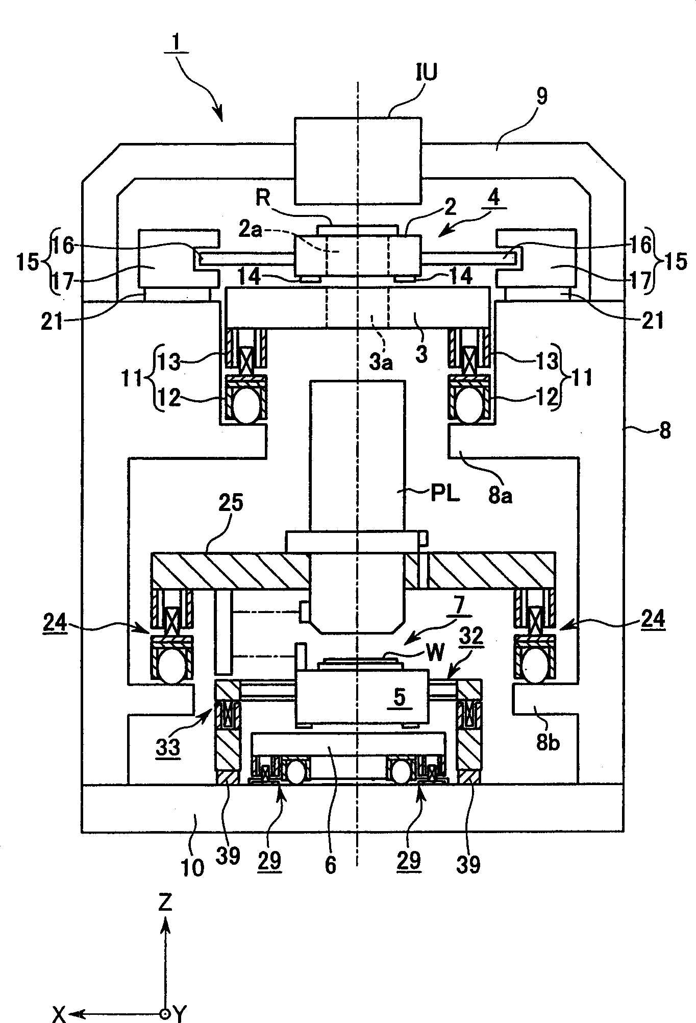
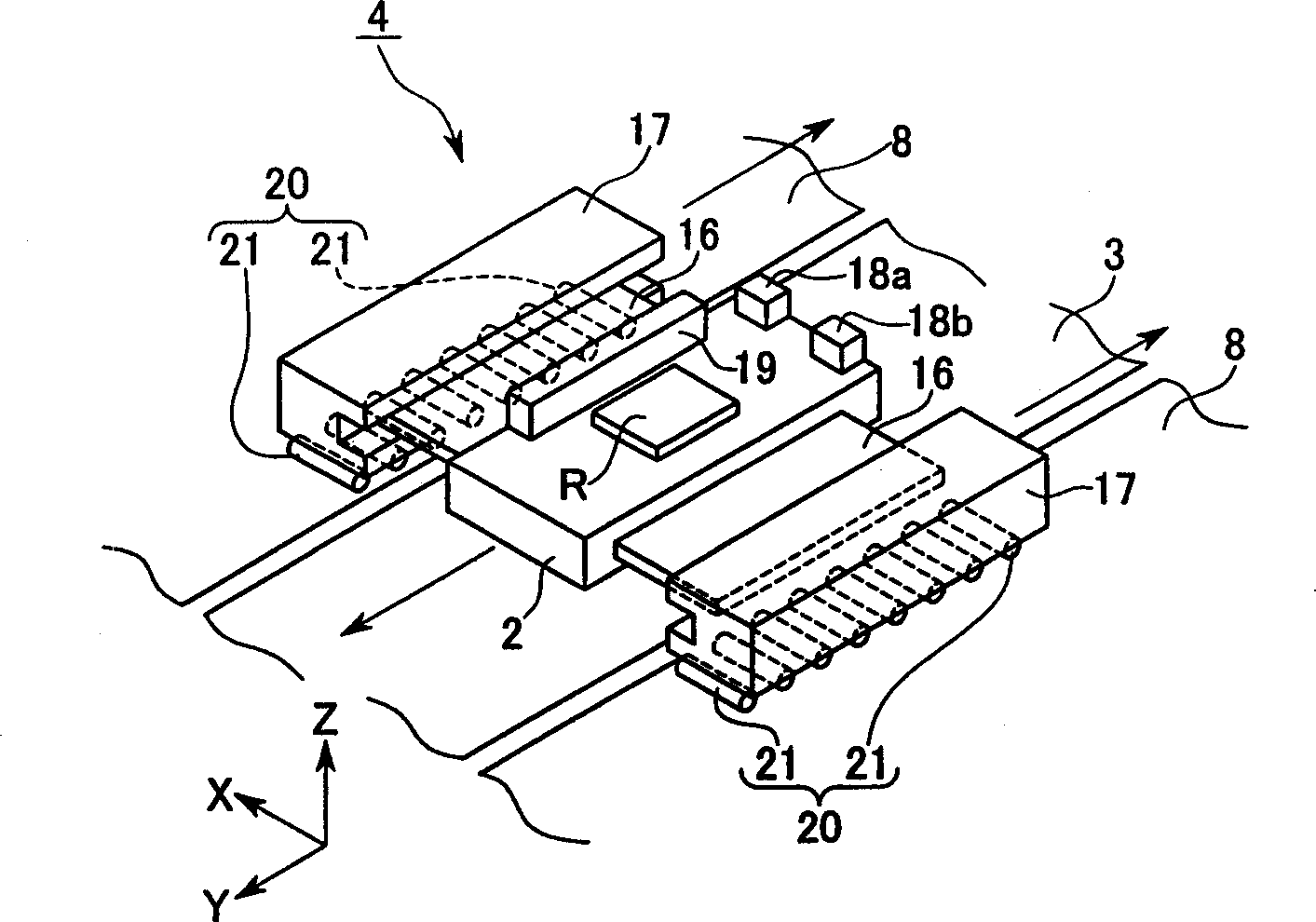
[0028] First, according to Figure 1 to Figure 5 The first embodiment will be described. figure 1 The shown exposure apparatus 1 is roughly configured as follows: a rectangular (or arc-shaped) illumination area on a regrind (mask) R is illuminated with uniform illuminance by exposure illumination light from a light source (not shown). Illumination optical system IU of the illumination optical system; comprise the original plate stage (stage body, the first object stage) 2 as the mask stage of holding original plate R and the original plate fixed disk (fixed disk) supporting this original plate stage 2 ) 3 stage device 4; projection optical system PL for projecting illumination light emitted from reticle R onto wafer (substrate) W; including wafer stage (stage Main body, first stage) 5 and stage device 7 holding wafer fixed plate (fixed plate) 6 of the wafer stage 5; and reaction frame supporting the above-mentioned stage device 4 and supporting projection optical system PL ...
no. 2 Embodiment
[0066] Figure 6 It is a figure which shows the 2nd Example of the stage apparatus and exposure apparatus of this invention. In this figure, with Figure 1 to Figure 5 The components that are the same as those of the first embodiment shown are assigned the same reference numerals, and description thereof will be omitted. The difference between the second embodiment and the above-mentioned first embodiment lies in the structure of the stage device 7, so it will be described below.
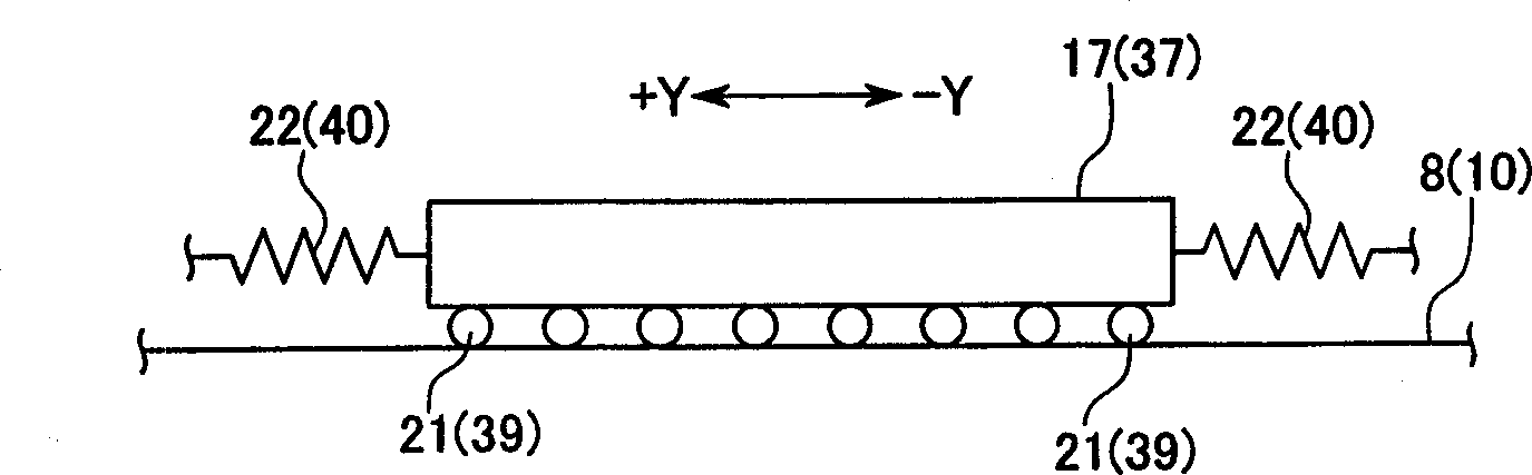
[0067] As shown in the figure, the stage device 7 is mainly composed of a wafer stage 5, a wafer holding plate 6, and a support frame (reaction stage) 46 supporting them from below. Furthermore, the stator 37 is configured to move in the Y direction with respect to the support frames 46 via the rotation rails 38 inserted between the support frames 46 . The wafer platen 6 is also vibrated independently of the support frames 46 by the anti-vibration unit 29 arranged between the support frames 46 . ...
no. 3 Embodiment
[0071] Figure 7 It is a figure which shows the 3rd Example of the stage apparatus and exposure apparatus of this invention. In this figure, with Figure 1 to Figure 5 The components that are the same as those of the first embodiment shown are assigned the same reference numerals, and description thereof will be omitted. The difference between the third embodiment and the above-mentioned first embodiment lies in the structure of the wafer stage 5, so it will be described below.
[0072] As shown in the figure, on both sides of the projection optical system PL in the Y direction, off-axis alignment sensors 49a, 49b are arranged at predetermined intervals, and the alignment sensors 49a, 49b are provided with two wafer stages 5 along the alignment direction. , 5. In each wafer stage 5, a magnet assembly (see figure) constituting a rotor of a movable linear motor is incorporated. Moreover, the linear guide rails 50 extending along the X direction of the stator of the wafer sta...
PUM
 Abstract
Description
Claims
Application Information