Integrated optical device and method of formation

A technology of Bragg gratings and substrates, applied in optics, optical components, light guides, etc., can solve problems such as expensive and complicated manufacturing processes

Inactive Publication Date: 2003-04-23
CORNING INC
View PDF0 Cites 8 Cited by
  • Summary
  • Abstract
  • Description
  • Claims
  • Application Information

AI Technical Summary

Problems solved by technology

Second, the manufacturing process of cur...

Method used


Image

  • Integrated optical device and method of formation
  • Integrated optical device and method of formation
  • Integrated optical device and method of formation

Examples


Embodiment Construction

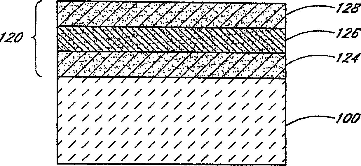
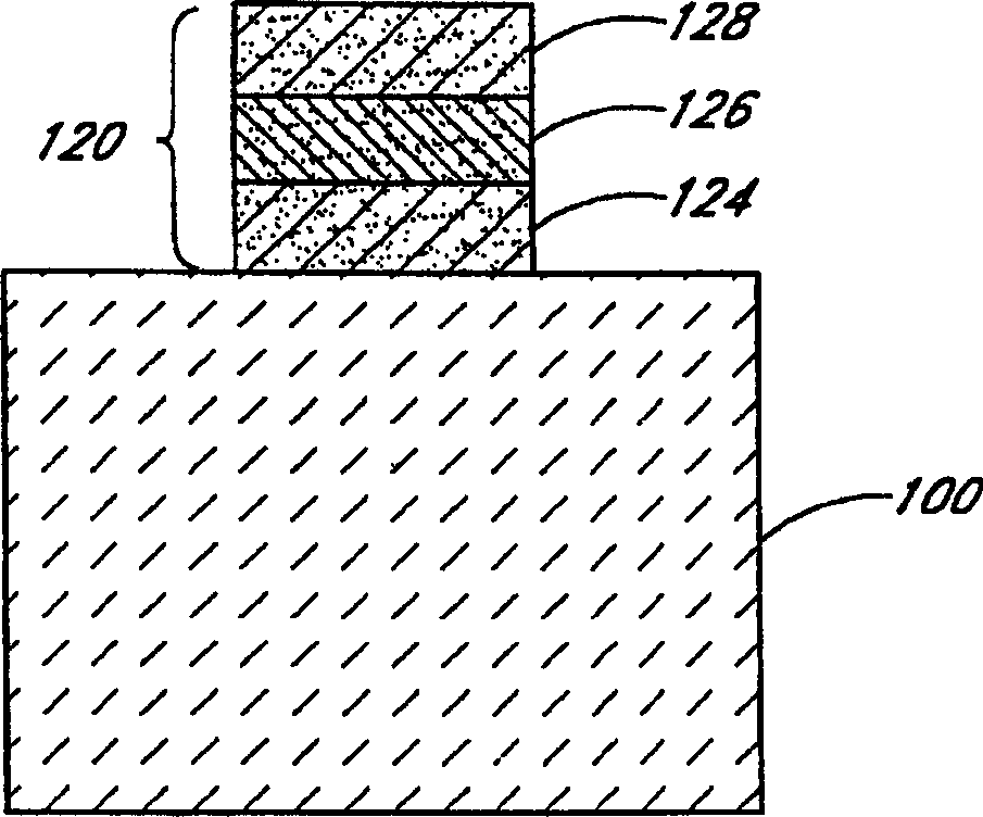
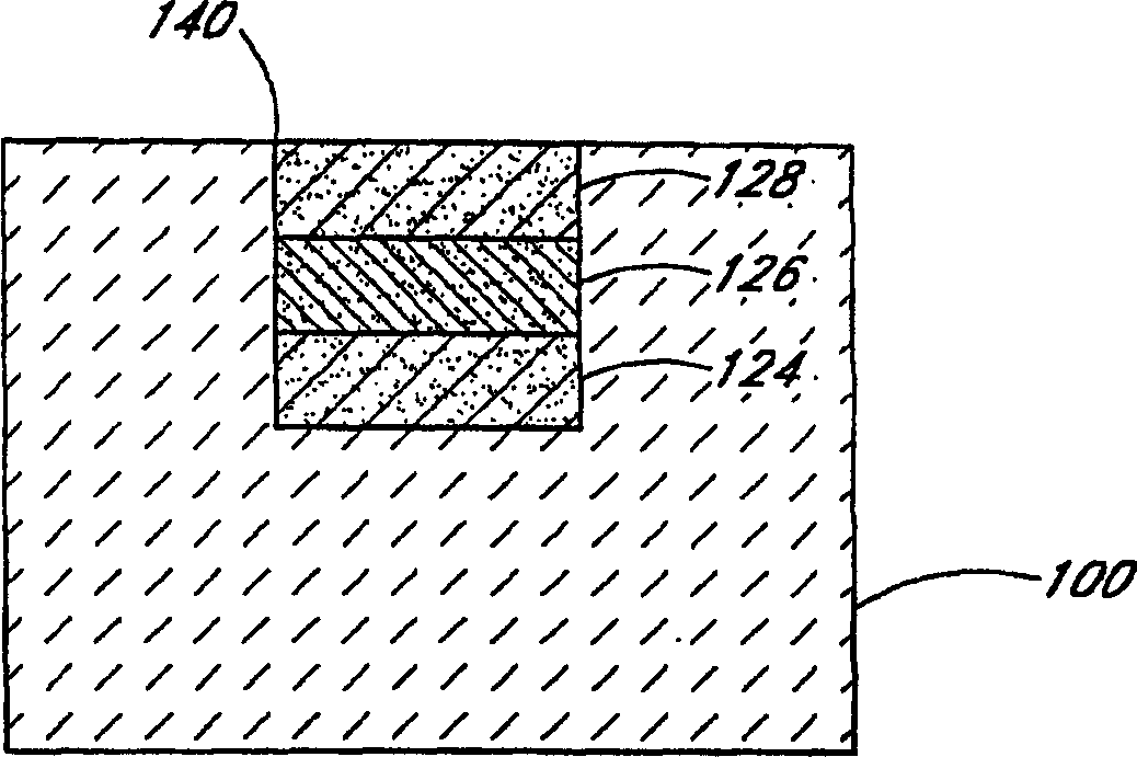
[0014] Such as figure 1 As mentioned above, the integrated planar Bragg grating includes a substrate 100 and a planar waveguide 120 . The substrate 100 includes a negative expansion material, that is, the substrate has a negative coefficient of thermal expansion. Preferably, the top surface of substrate 100 is polished, which includes a glass-ceramic material, such as lithium aluminum silicate (eg, β-eucryptite). Substrate 100 preferably comprises an amorphous material. Waveguide 120 is formed on substrate 100 by alternately depositing material on the substrate and reducing stress in the deposited material. In the disclosed preferred embodiment, the waveguide includes a cladding 124 formed by depositing a series of thin layers on a substrate. For example, a quartz film with a thickness of 0.1 micron may be deposited on the substrate 100, and then the stress in the deposited film may be reduced through an annealing cycle. Annealing of the cladding 124 also provides a stron...


PUM


Abstract

An integrated planar Bragg grating is fabricated by depositing layers of material onto a negative expansion substrate to form a waveguide, which is held in mechanical tension with the substrate. A Bragg grating is then formed in the waveguide. As the temperature of the waveguide increases, the mechanical tension between the waveguide and the substrate is relieved, such that the peak reflection wavelength of the Bragg grating remains nearly constant.

Description

Background of the invention [0001] 1. technical field [0002] The present invention relates generally to integrated optical ("planar") Bragg gratings, and more particularly, to integrated optical Bragg gratings whose peak reflection wavelength is substantially insensitive to temperature changes. [0003] 2. Background technique [0004] A Bragg grating comprises an optical waveguide defining a pattern or stack of regions of alternating higher and lower refractive indices, so that the grating reflects light in a narrow wavelength band and wavelengths outside the band are transmitted through the grating. Bragg gratings are good narrowband filters for various applications such as wavelength multiplexers, fiber laser mirrors, dispersion control devices or sensors. For this reason, Bragg gratings are becoming more and more important in optical communications. [0005] An important characteristic of a Bragg grating is the stability of its peak reflection wavelength with res...

Claims


Application Information

Patent Timeline
IPC IPC(8): G02B6/122C03C17/34G02B5/18G02B6/12G02B6/124G02B6/13G02B6/132
CPCG02B2006/12176Y10S359/90C03C17/3417G02B6/132G02B6/124G02B2006/12169C03C17/3411
Inventor A·K·加德卡瑞K·P·加德卡瑞
Owner CORNING INC
Why Eureka
Try Eureka