Optical mounting substrate and optical device

A technology for installing substrates and optical devices, applied to optics, optical components, optical waveguides and light guides, etc., can solve problems such as not being installed in the correct position and weakening the advantages of costs

Inactive Publication Date: 2003-06-11
PANASONIC CORP
View PDF3 Cites 21 Cited by
  • Summary
  • Abstract
  • Description
  • Claims
  • Application Information

AI Technical Summary

Problems solved by technology

Especially in the case of using an optical fiber that is processed to have a slanted end, if the optical fiber is not installed in the correct orientation due to rotation or the like, the light output from the optical fiber may not be properly incident on the photodiode
[0014] Thus, although conventional optical device structures have the advantage of simplifying aspects related to photodiode mounting, they require additional processing steps, which diminishes the cost advantage

Method used


Image

  • Optical mounting substrate and optical device
  • Optical mounting substrate and optical device
  • Optical mounting substrate and optical device

Examples


no. 1 example

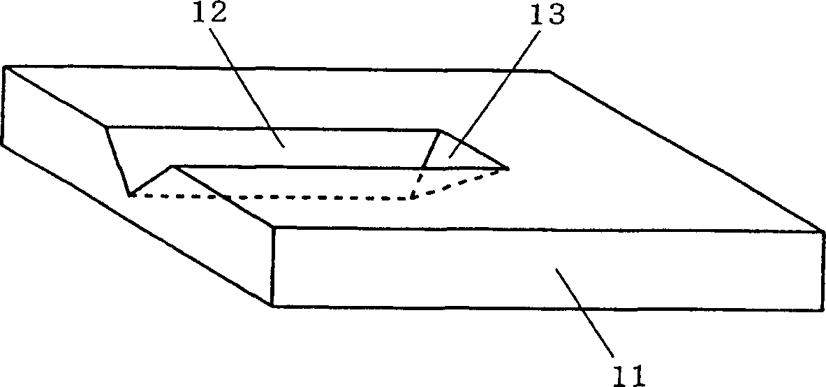
[0064] figure 1 is a perspective view showing the structure of the optical mounting substrate 11 according to the first embodiment of the present invention. Such as figure 1 As shown, a guide groove 12 for positioning an optical fiber is formed on the surface of an optical mounting base 11 , wherein a tapered surface 13 is formed adjacent to the guide groove 12 . The tapered surface 13 forms a predetermined angle with respect to the surface of the optical mounting substrate 11 .

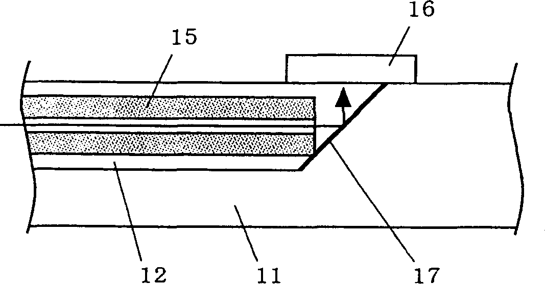
[0065] figure 2 is a cross-sectional view, which shows the use of figure 1 An optical device of an optical mounting substrate 11 on which an optical fiber 15 and a surface-receiving photodiode 16 are mounted.

[0066] Such as figure 2 As shown, the optical device structure using the optical mounting substrate 11 includes a mirror 17 formed on a tapered surface 13 formed of a thin film capable of reflecting light. The optical fiber 15 is attached in the guide groove 12 using, for example, a...

no. 2 example

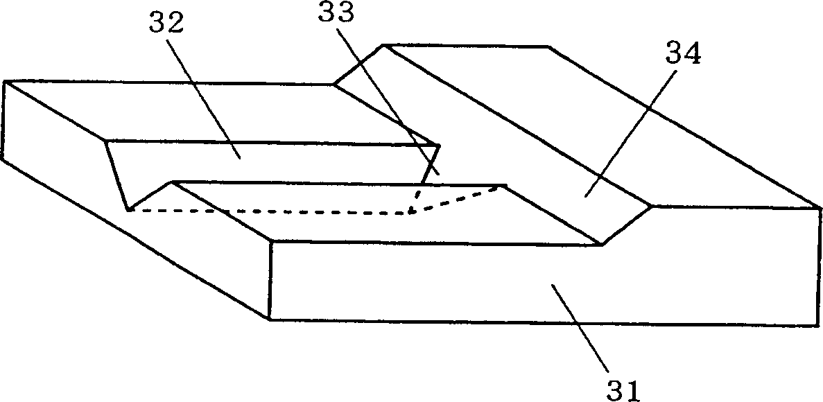
[0074] image 3 is a perspective view showing the structure of an optical mounting substrate 31 according to a second embodiment of the present invention. Such as image 3As shown, a guide groove 32 for positioning an optical fiber is formed on a surface of an optical mounting base 31, and a tapered surface 33 is formed adjacent to the guide groove 32. The tapered surface 33 forms a predetermined angle with respect to the surface of the optical mounting substrate 31 . The surface of the mounting base 31 bends at the slope 34 .

[0075] Figure 4 is a cross-sectional view, which shows the use of image 3 Shown is an optical device of an optical mounting base 31, wherein an optical fiber 35 and a surface-receiving photodiode 36 are mounted on the optical mounting base.

[0076] exist Figure 4 In the shown optical device using the optical mounting substrate 31, on the tapered surface 33, a diffraction grating 37 for diffracting light is provided. The optical fiber 35 is a...

no. 3 example

[0084] Figure 5 is a perspective view showing the structure of an optical mounting substrate 51 according to a third embodiment of the present invention. Such as Figure 5 As shown, a guide groove 52 for positioning the optical fiber is formed on the surface of the optical mounting base 51, and a predetermined tapered surface 53 is formed adjacent to the guide groove 52.

[0085] Figure 6 is a cross-sectional view, which shows the use of Figure 5 Shown is an optical device of an optical mounting base 51 on which an optical fiber 55 and a surface-emitting laser 56 are mounted.

[0086] Such as Figure 6 As shown, the optical device structure using the optical mounting substrate 51 includes a tapered surface 53 having a lens-like curvature, and a mirror 57 is formed of a film capable of reflecting light formed on the tapered surface 53 . The optical fiber 55 is attached in the guide groove 52 . The optical fiber 55 is only required to be placed in the guide groove 52, b...


PUM


Abstract

There is provided an optical package substrate and a molding method therefor, which provides for easy production, easy mounting of optical elements such as photodiodes and lasers, good functionality, productivity, and economy, as well as an optical device incorporating the package substrate. On the surface of an optical package substrate 11, a guide groove 12 used for the positioning of an optical fiber and a tapered face 13 adjoining the guide groove 12 are provided, the tapered face 13 being formed so as to have a predetermined angle. A mirror 17 for reflecting light is formed on the tapered face 13. An optical fiber 15 is affixed in the guide groove 12. Above the tapered face 13 is mounted a surface reception type photodiode 16, which is placed in a position for receiving light deflected by the mirror 17 provided on the tapered face 13. By providing a positioning marker (not shown) for a light receiving element on the optical package substrate 11, it becomes particularly easy to mount the surface reception type photodiode 16 through passive alignment.

Description

(1) Technical field [0001] The present invention relates to an optical mounting substrate (optical package substrate) and an optical device thereof, and more particularly to a mounting substrate having a surface structure suitable for mounting optical components and or optical elements and a molding method of the mounting substrate thereof, and An optical device constructed using this mounting base. (2) Background technology [0002] Optical communication systems using optical fibers are developing from traditional long-distance communication systems to user communication systems. Subscriber optical communication systems require the use of small and inexpensive optical devices. [0003] In conventional optical devices, optical components such as optical fibers and / or lenses and optical elements such as lasers and / or photodiodes are arranged coaxially. Usually, the positioning of optical fibers and lenses requires high precision, for example, a tolerance of ±1 micron. Acco...

Claims


Application Information

Patent Timeline
Patent Type & Authority Applications(China)
IPC IPC(8): G02B6/12G02B6/122G02B6/13G02B6/42H01L31/0232H01S5/022
CPCG02B6/42G02B6/4214G02B6/423G02B6/12
Inventor 是永继博伊藤伸器东城正明和田纪彦
Owner PANASONIC CORP
Why Eureka
Try Eureka