Display device having initalzing function to brightness data of optical element

A technology for optical components and display devices, applied in optics, electrical components, nonlinear optics, etc., and can solve problems such as residual images and inability to accurately set brightness data.

Inactive Publication Date: 2003-07-02
SANYO ELECTRIC CO LTD
View PDF1 Cites 27 Cited by
  • Summary
  • Abstract
  • Description
  • Claims
  • Application Information

AI Technical Summary

Problems solved by technology

[0007] When the luminance data set for an optical element is large, attempts to set smaller luminance data by overwriting the luminance data often result in the phenomenon of residual images, in which the charge associated with the previously larger luminance data is not completely removed. remain in the optics and therefore cannot accurately set the desired luminance data

Method used


Image

  • Display device having initalzing function to brightness data of optical element
  • Display device having initalzing function to brightness data of optical element
  • Display device having initalzing function to brightness data of optical element

Examples


Embodiment Construction

[0028] The present invention will now be described according to a preferred embodiment, the use of which is not to limit the scope of the invention but to illustrate the invention. All features and combinations thereof described in the exemplary embodiments are not absolutely essential to the invention.

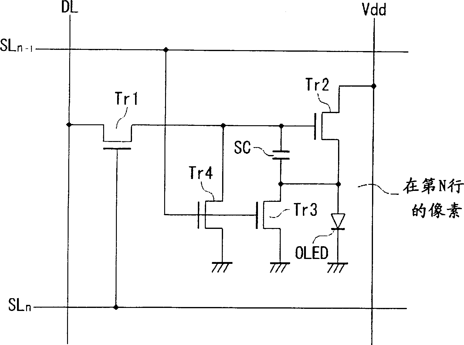
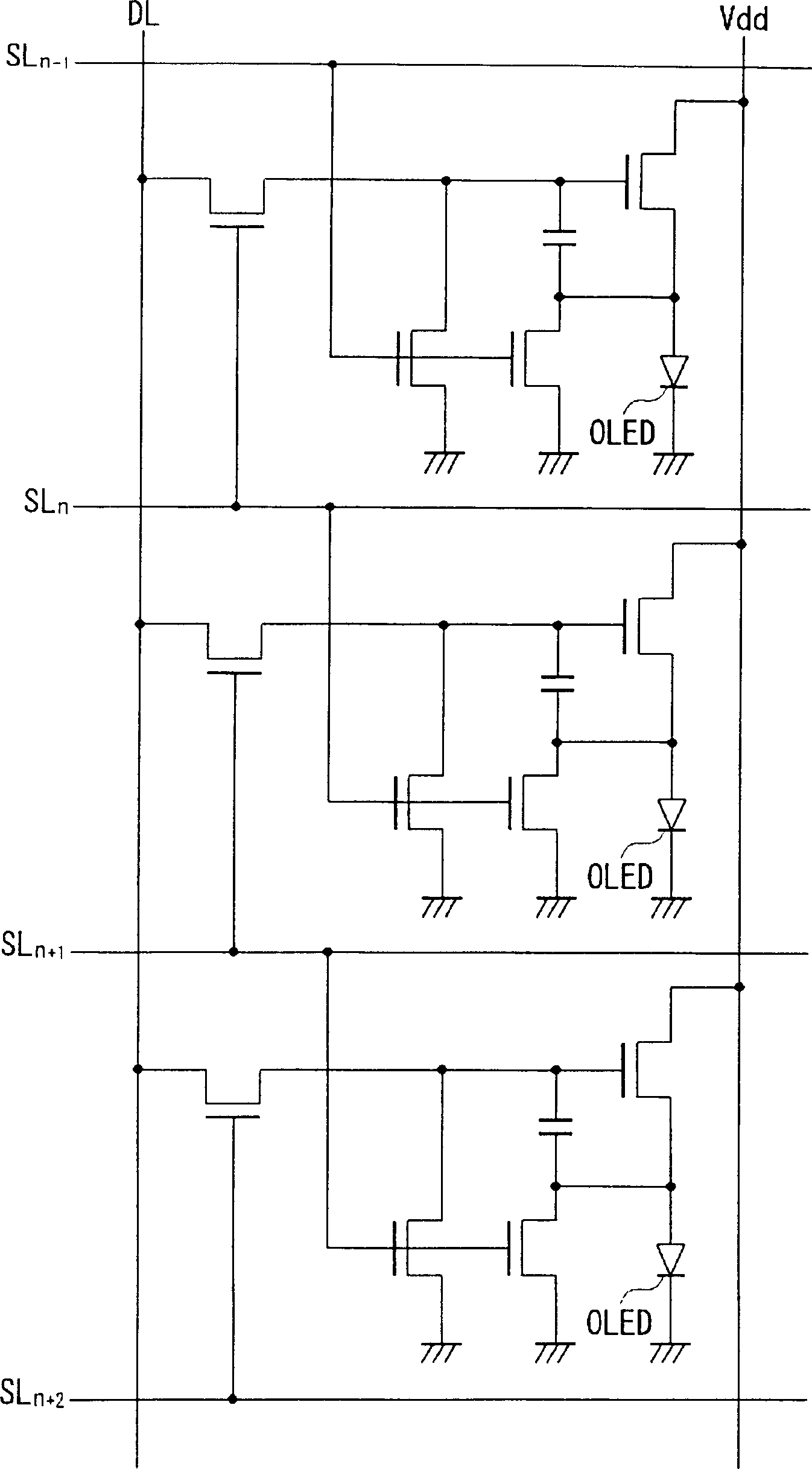
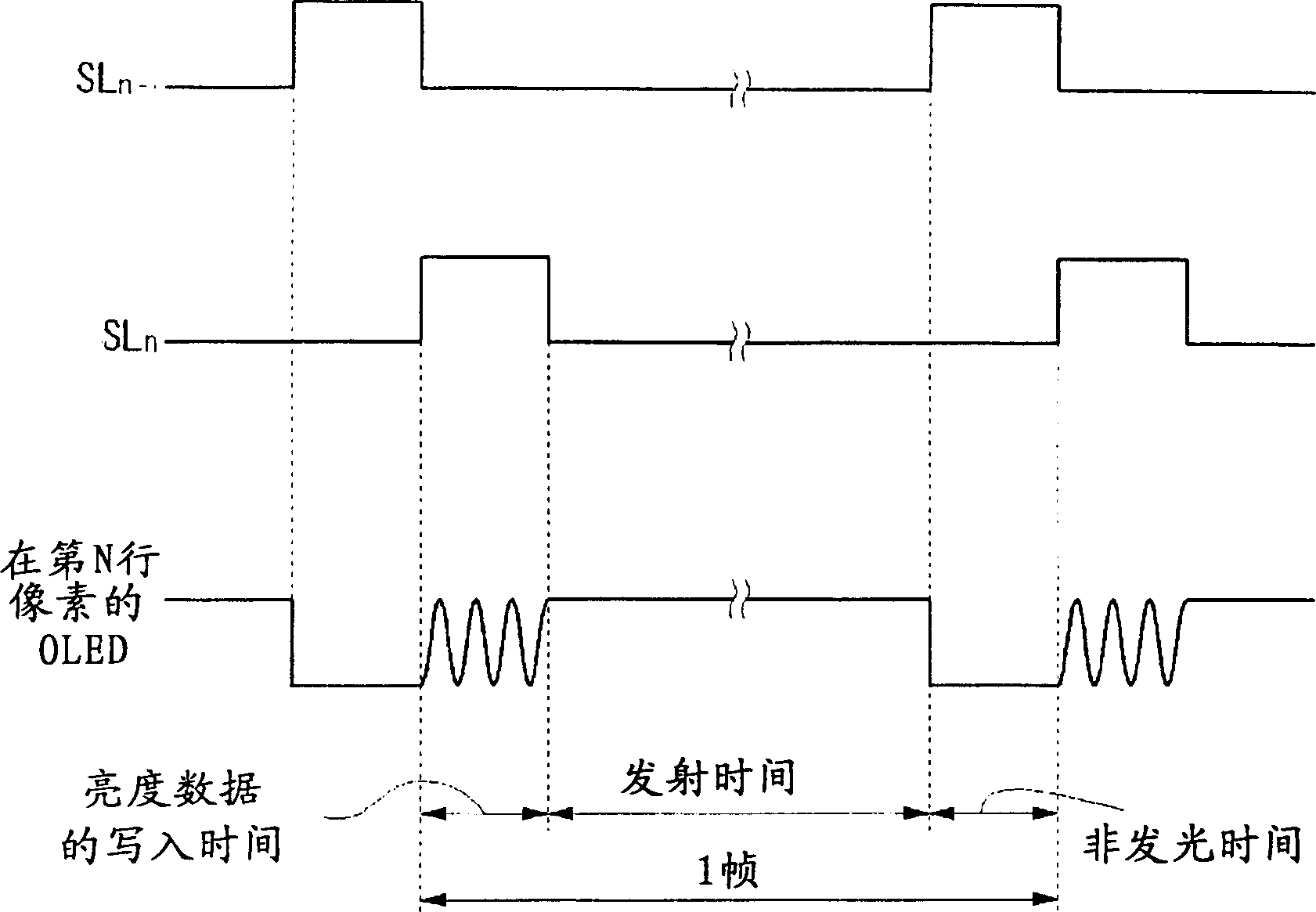
[0029] In the following embodiments, an active matrix organic EL (Electro Luminescence) display is assumed as a display device, and an organic light emitting diode is assumed as an optical element. In these embodiments, novel circuits that can reduce the above-mentioned image sticking phenomenon will be proposed. Therefore, the bypass including the switching element is arranged in parallel from the anode of the optical element to the ground potential. Another switching element is also provided between the gate electrode of the drive transistor and ground potential. By switching these switching elements immediately before the scan signal of the pixel line, the luminance data...


PUM


Abstract

Prior to writing new luminance data in the n-th row pixel, as the (n-1)th scanning line turns high to write the luminance data in the (n-1)th row pixel, the bypass transistor and the initialization transistor of the n-th row pixel turn on. Hence, the luminance data having been set in the driving transistor is initialized, and the organic light emitting diode goes out.

Description

technical field [0001] The present invention relates to a display device, and more particularly to a technique for improving display quality of an active matrix type display device. Background technique [0002] The use of notebook personal computers and portable terminals is spreading rapidly. The displays mainly used in such devices are liquid crystal displays, but the displays considered promising as next-generation flat display panels are organic EL (Electro-Luminescence) displays. And the active matrix driving system is very important for the display method of this kind of display. A display using this system is called an active matrix display, in which a plurality of pixels are arranged vertically and horizontally in a matrix, and a switching element is provided for each pixel. Image data is sequentially written into each pixel through the switching element. [0003] Today's research and development for designing a practical organic EL display is in the development ...

Claims


Application Information

Patent Timeline
Patent Type & Authority Applications(China)
IPC IPC(8): G02F1/1368G02F1/133G09G3/20G09G3/30G09G3/32H01L51/50
CPCG09G2300/0861G09G2300/0842G09G2300/0814G09G2320/043G09G2300/0809G09G2310/0251G09G2320/0257G09G2320/0252G09G3/3233G09G2310/0254G09G2310/0256G09G3/20
Inventor 山田光一
Owner SANYO ELECTRIC CO LTD
Why Eureka
Try Eureka