Chip pick-up device and producing method thereof and production apparatus of semiconductor

A technology for picking up devices and chips, which is applied in semiconductor/solid-state device manufacturing, electrical components, electrical components, etc., and can solve the problem that the chip 102 is not easy to peel off

Inactive Publication Date: 2003-08-20
SHARP KK
View PDF0 Cites 11 Cited by
  • Summary
  • Abstract
  • Description
  • Claims
  • Application Information

AI Technical Summary

Problems solved by technology

[0011] but, Figure 9 In the shown device, the pinholes 131b and the suction holes 131c are connected inside the stage 131, so the air is also sucked through the pinholes 131b, in fact as Figure 10 As shown, the pape

Method used


Image

  • Chip pick-up device and producing method thereof and production apparatus of semiconductor
  • Chip pick-up device and producing method thereof and production apparatus of semiconductor
  • Chip pick-up device and producing method thereof and production apparatus of semiconductor

Examples


Embodiment Construction

[0045] Hereinafter, embodiments of the present invention will be described in detail with reference to the drawings.

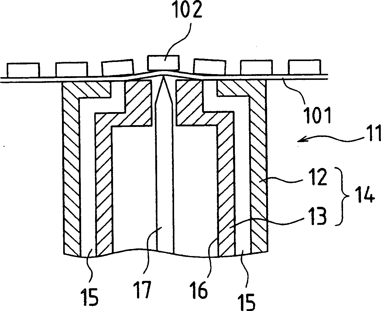
[0046] figure 1 It is a partial cross-sectional view showing one embodiment of the pickup device of the present invention. In the pick-up device 11 of the present embodiment, a cylindrical body 12 is erected, and a needle holder 13 is disposed inside the cylindrical body 12 to constitute a stage 14 . A gap is formed between the inner periphery of the cylindrical body 12 and the outer periphery of the needle holder 13, and this gap is used as a suction vent hole 15 for air. A needle hole 16 is formed in the needle holder 13 , and a needle 17 is inserted into the needle hole 16 .

[0047] The suction vent hole 15 is connected to a vacuum pump (not shown), and the air in the suction vent hole 15 is sucked by the vacuum pump. The pinholes 16 are formed completely apart from the suction vent holes 15, so the air in the pinholes 16 will not be sucked.

[0048] ...


PUM


Abstract

The present invention relates to a chip pickup device capable of easily peeling off chips from a passivation layer without having to particularly adjust the push-up stroke of a pushing pin and the ascending/descending position of a supporting stage. The pushing pin 17 is protruded out of a pin hole 16. The pushing pin 17 is used to push a chip 102 via a passivation layer 101. The passivation layer 101 is sucked and drawn near the venting hole 15, but is not sucked and drawn near the pin hole 16. The passivation layer 101 is propped up at the vicinity of the pin hole 16 to be separated from the supporting stage 14, thereby peeling off the chip 102 from the passivation layer 101. Therefore, it is able to keep the stroke of the pushing pin 17 constant without modifying or adjusting the position of the supporting stage 14. In addition, because there is no absorbing force of air in the pin hole 16, it is easy to peel off the chip 102 from the passivation layer 101.

Description

field of invention [0001] The present invention relates to a chip pickup device, a manufacturing method thereof, and a semiconductor manufacturing device for supplying chips to electronic components and the like. Background technique [0002] Existing devices of this type include, for example, devices shown in Fig. 6(a) and (b). This device uses the needle 103 to pass through the paper 101 to push up the chips 102 of electronic components and the like pasted on the paper 101, so that the chip 102 is peeled off from the paper 101, and then absorbs and picks up the chip 102 with an opening clip (not shown). 102 is provided to the die-bonding head etc. of the die-bonding device. [0003] In addition, as shown in Fig. 7 (a) and (b), the paper 101 is covered on the inner cylindrical ring 111, and in the state where the paper 101 is spread out, the outer cylindrical ring 112 is fitted to the inner cylindrical ring. 111, the outer edge of the paper 101 is clamped to support it, a...

Claims


Application Information

Patent Timeline
IPC IPC(8): H01L21/683H01L21/50H01L21/68H05K13/00
Inventor 孝桥生郎
Owner SHARP KK
Why Eureka
Try Eureka