Semiconductor manufacturing device, semiconductor manufacturing system and substrate processing method

A technology for manufacturing devices and processing methods, which is applied in semiconductor/solid-state device manufacturing, comprehensive factory control, comprehensive factory control, etc., and can solve problems such as huge investment

Inactive Publication Date: 2003-10-01
KK TOSHIBA
View PDF0 Cites 10 Cited by
  • Summary
  • Abstract
  • Description
  • Claims
  • Application Information

AI Technical Summary

Problems solved by technology

In addition, for the enlargement of such supply equipment and conveying equipment, a huge investment is required

Method used


Image

  • Semiconductor manufacturing device, semiconductor manufacturing system and substrate processing method
  • Semiconductor manufacturing device, semiconductor manufacturing system and substrate processing method
  • Semiconductor manufacturing device, semiconductor manufacturing system and substrate processing method

Examples


no. 1 Embodiment approach

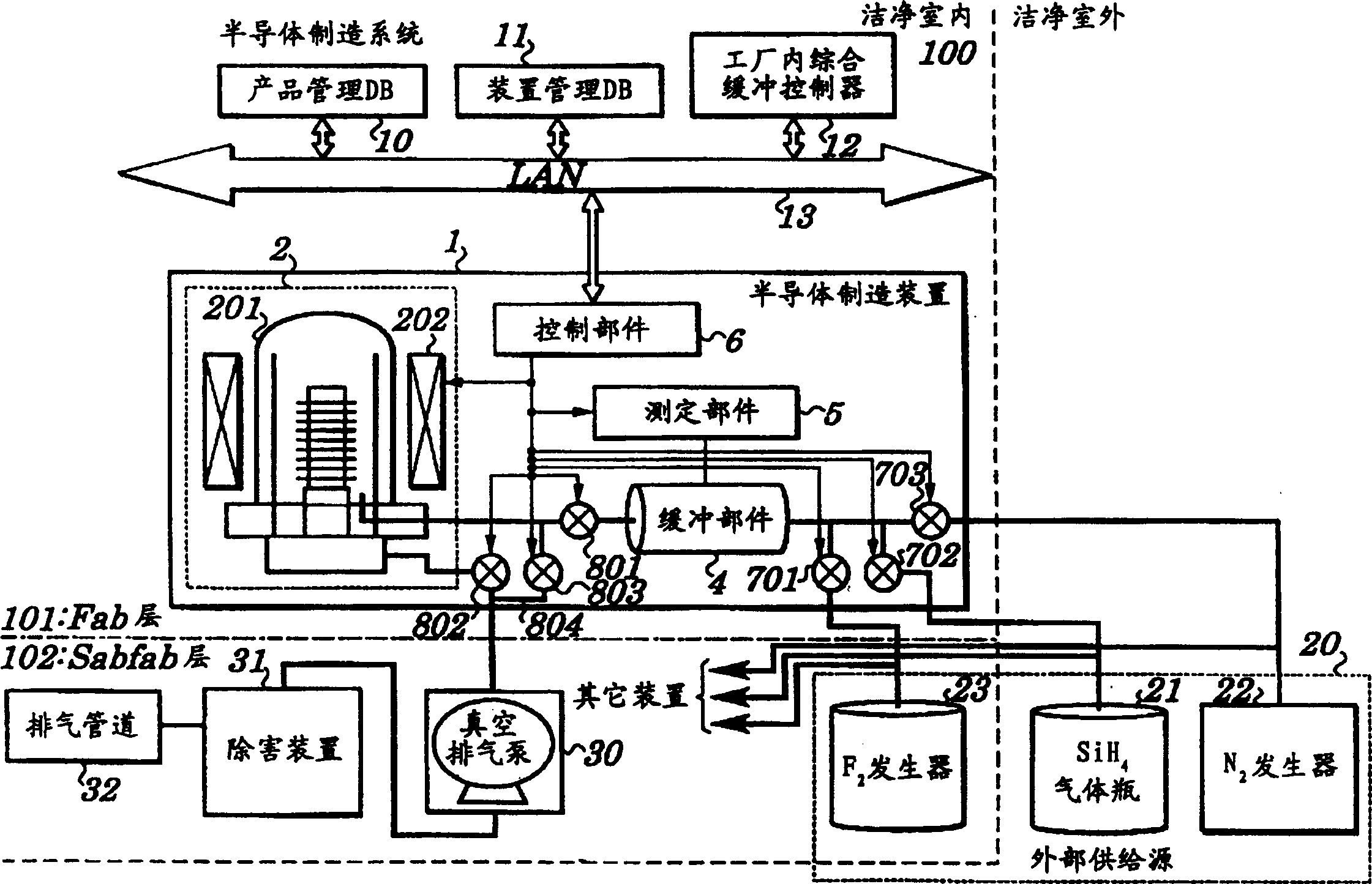
[0047] In a first embodiment of the present invention, an LPCVD apparatus is used as a semiconductor manufacturing apparatus, and the present invention is applied to the semiconductor manufacturing apparatus, a semiconductor manufacturing system composed of the semiconductor manufacturing apparatus, and a substrate processing method used therefor.

[0048] Basic structure of semiconductor manufacturing equipment and semiconductor manufacturing system

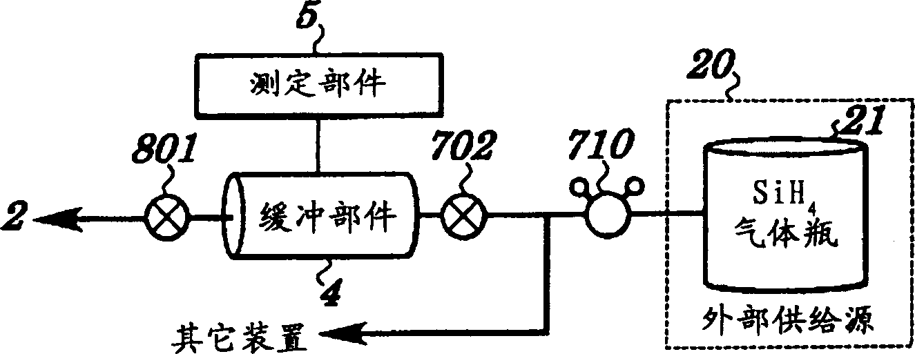
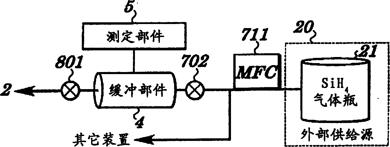
[0049] Such as figure 1 As shown, the semiconductor manufacturing apparatus 1 according to the first embodiment of the present invention is an LPCVD apparatus for forming a polysilicon film on the surface of a semiconductor wafer using monosilane gas as a material gas. That is, the semiconductor manufacturing apparatus 1 includes at least a processing chamber 2 for performing substrate processing, supplies materials necessary for processing from an external supply source 20 to the inside of the processing chamber 2 or the inside...

no. 2 Embodiment approach

[0127] The second embodiment of the present invention is an example in which the buffer member 4 built in the semiconductor manufacturing apparatus 1 constituting the first embodiment of the present invention is described as an external semiconductor manufacturing apparatus.

[0128] Such as Figure 13 As shown, in the semiconductor manufacturing system according to the second embodiment of the present invention, unlike the semiconductor manufacturing apparatus 1 having the processing chamber 2, an additional semiconductor manufacturing apparatus 1A is arranged. The semiconductor manufacturing apparatus 1A includes a buffer member 4 that supplies substances necessary for substrate processing from an external supply source 20 , stores the supplied substances, and supplies the stored substances to the outside, that is, the processing chamber 2 of the semiconductor manufacturing apparatus 1 .

[0129] Further, the semiconductor manufacturing apparatus 1A includes a control unit 6...

no. 3 Embodiment approach

[0133] Third Embodiment of the Present Invention An example in which the present invention is applied to the semiconductor manufacturing apparatus 1 and the semiconductor manufacturing system according to the first embodiment of the present invention will be described in terms of a method for cleaning the inner wall of the reaction tube 201 in the processing chamber 2 of the semiconductor manufacturing apparatus 1 .

[0134] basic cleaning method

[0135] In the reaction tube 201 of the semiconductor manufacturing apparatus 1 according to the first embodiment of the present invention, a polysilicon film is formed by LPCVD according to the previous example, so the method for cleaning the silicon film adhering to the inner wall of the reaction tube 201 will be described here. Also, here, using figure 1 Be explained. Furthermore, the process of forming a silicon film on a semiconductor wafer is a direct substrate process, but the process of cleaning the silicon film adhering to ...


PUM


Abstract

The present invention provides a semiconductor manufacturing device, a semiconductor manufacturing system, and a semiconductor manufacturing device, a semiconductor manufacturing system, and a substrate that can supply only a required amount of liquid, gas, or solid used directly or indirectly in substrate processing when necessary, and can realize miniaturization of supply equipment or conveying equipment. Bottom treatment method. The semiconductor manufacturing apparatus 1 and the semiconductor manufacturing system include a buffer member 4 . The buffer member 4 temporarily stores substances required for substrate processing supplied from the external supply source 20 , and supplies the stored substances to the processing chamber 2 . The supply of the substance is controlled by the CIM through the control unit 6 and the LAN 13 .

Description

technical field [0001] The invention relates to a semiconductor manufacturing device, a semiconductor manufacturing system and a substrate processing method. In particular, the present invention relates to a semiconductor manufacturing device provided with a supply system for supplying materials required for processing to the inside of a processing chamber for substrate processing, a semiconductor manufacturing system constructed by at least including a supply system and a semiconductor manufacturing device, and the use of the semiconductor manufacturing device and substrate processing methods for semiconductor manufacturing systems. Background technique [0002] In semiconductor manufacturing equipment, various material gases, chemicals, solvents, etc. are used in accordance with the steps of the semiconductor device manufacturing process. Generally speaking, these material gases, chemical liquids, solvents, etc. are supplied from a small cylindrical tank adjacent to a sem...

Claims


Application Information

Patent Timeline
Patent Type & Authority Applications(China)
IPC IPC(8): G05B19/418C25B9/00C25B11/00H01L21/00H01L21/205
CPCH01L21/67017Y02P90/02
Inventor 中尾隆宫崎邦浩
Owner KK TOSHIBA
Why Eureka
Try Eureka