Electronic device for supplying power source and noise filter which having high-efficient noise reducing

A technology of electronic devices and filters, applied in circuit devices, reduction of crosstalk/noise/electromagnetic interference (, electric solid-state devices, etc.), can solve problems such as impedance rise

Inactive Publication Date: 2003-10-01
TOKIN CORP
View PDF3 Cites 2 Cited by
  • Summary
  • Abstract
  • Description
  • Claims
  • Application Information

AI Technical Summary

Problems solved by technology

Also, the impedance of vias 9-12 increases as

Method used


Image

  • Electronic device for supplying power source and noise filter which having high-efficient noise reducing
  • Electronic device for supplying power source and noise filter which having high-efficient noise reducing
  • Electronic device for supplying power source and noise filter which having high-efficient noise reducing

Examples


no. 1 example

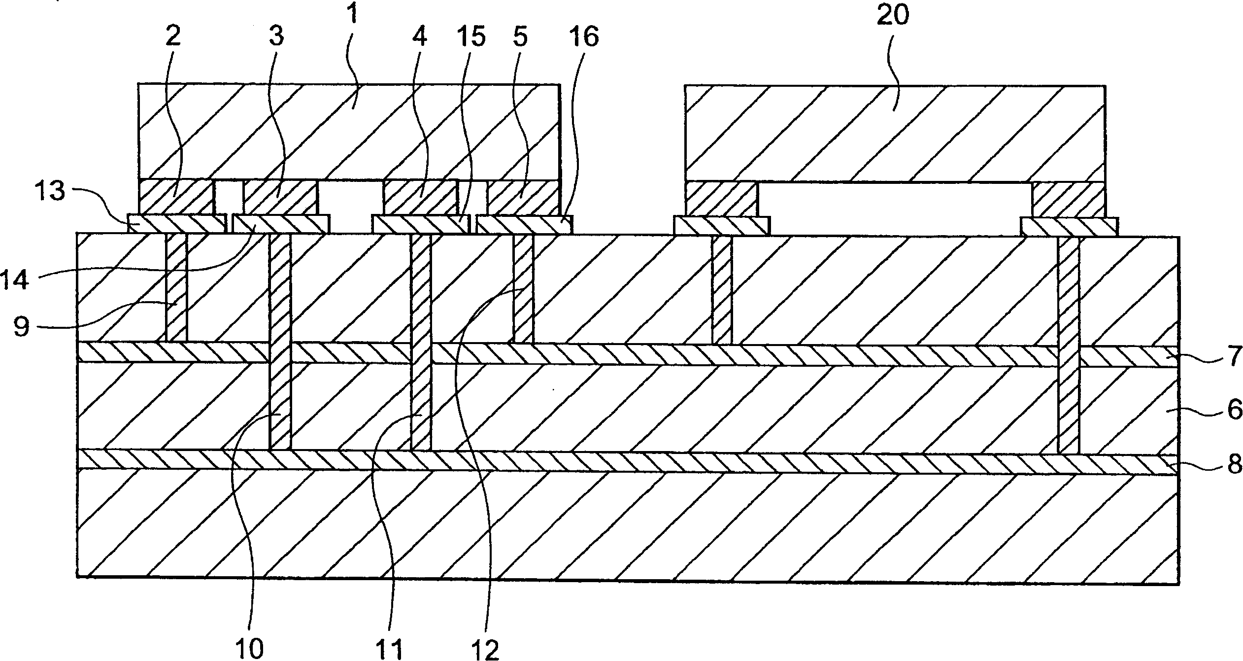
[0049] see image 3 , an electronic device includes a circuit board 6 and a noise filter 1 fixed on the circuit board. In this embodiment, a load circuit 20 such as an LSI chip is also mounted on the circuit board 6 .

[0050] The noise filter 1 has power and ground input terminals 2 and 3 and power and ground output terminals 5 and 4 .

[0051] The circuit board 6 has on its surface first to fourth conductor regions 13-16 connected to the power and ground input terminals 2 and 3 and the power and ground output terminals 5 and 4 of the noise filter 1, respectively. The circuit board 6 has a power line conductor layer (VCC layer) 7 a and a ground layer (GND layer) 8 a as independent internal conductive layers inside the circuit board 6 . The VCC layer 7a and the GND layer 8a extend to below the first and second conductor regions 13 and 14 respectively, and are connected to the first and second conductor regions through the first and second through holes 9 and 10, in the circu...

no. 2 example

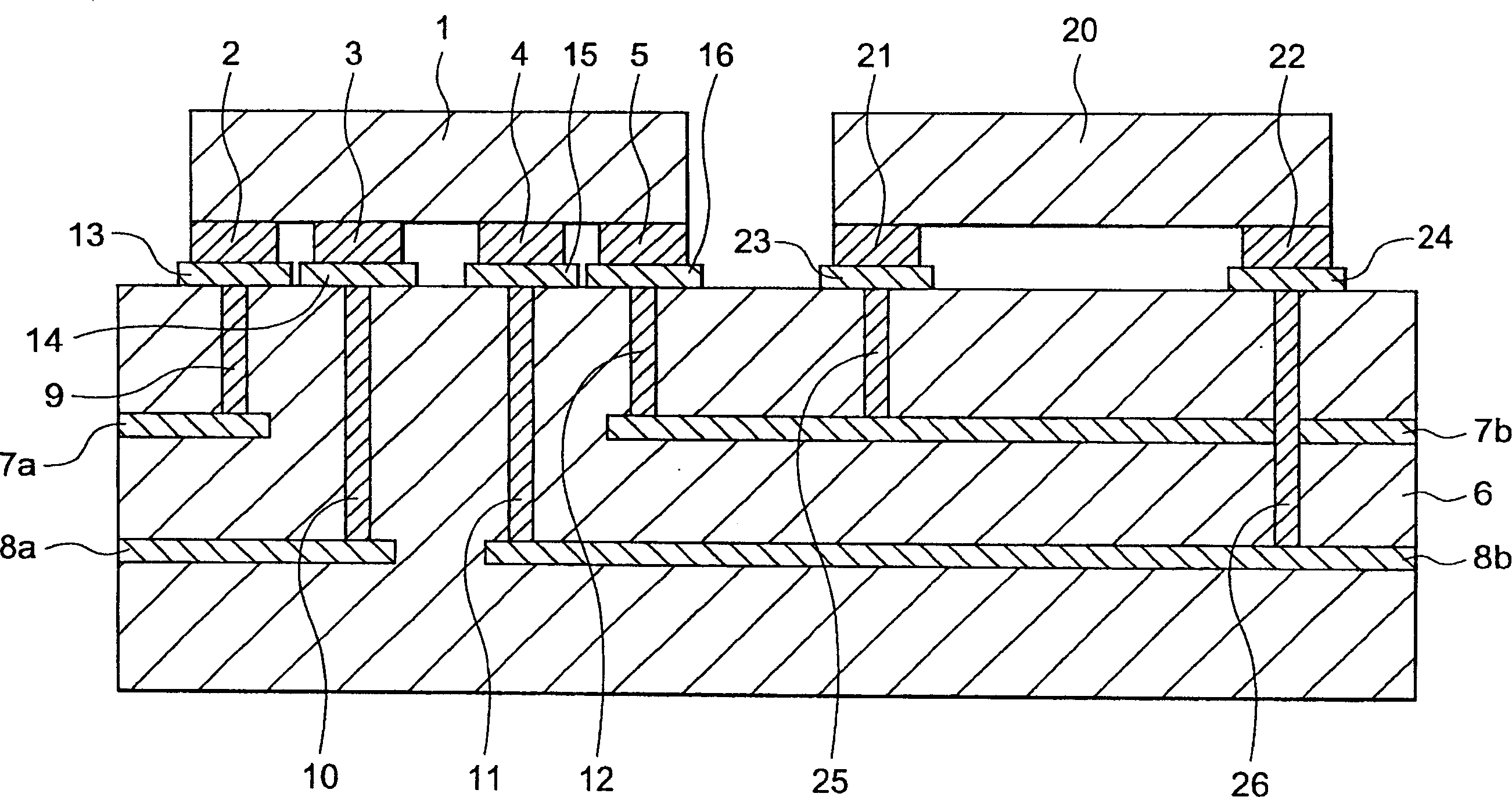
[0059] see Figure 4 , except that will be in image 3 The electronic device shown is similar to the first embodiment, except that the ground input and output terminals 3 and 4 are connected together to form a single ground terminal indicated only by reference numeral 3.

[0060] In this embodiment, those skilled in the art can understand that the Figure 4 electronics in the image 3 The embodiment shown in works in the same way.

no. 3 example

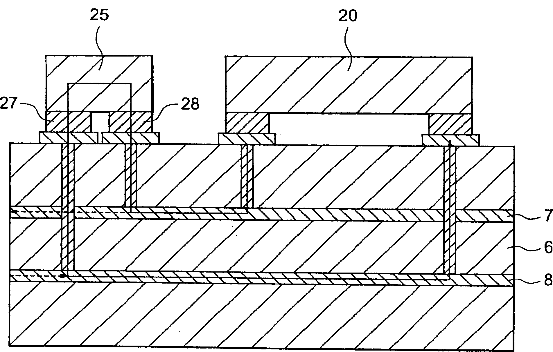
[0062] see Figure 5 , the electronic device according to the third embodiment shown here is an LSI chip 20 fixed on another circuit board 17 with a DC power supply. Another circuit board 17 has conductor areas 27 and 28 for receiving power supply terminals and ground terminals 21 and 22 of the LSI chip 20 mounted and connected to the circuit board 17 . On the other surface of the circuit board 17 there are further conductor areas 30 and 29 which are connected to the conductor areas 27 and 28 respectively.

[0063] In this embodiment, the circuit board 6 does not make the power supply conductor 7b and the ground conductor 8b the inner layer of the 0-VCC and 0-GND layers, but makes them such as 0-VCC pin 19 and 0-GND pin 18 conductive pins. The 0-VCC pin and the 0-GND pin are located above the fourth and third conductor regions 16 and 15 .

[0064] The 0-VCC pin 19 and the 0-GND pin 18 are connected to conductor areas 30 and 29 on another circuit board 17 . Therefore, the po...


PUM


Abstract

In an electronic device for supplying DC power to an LSI chip (20), a distributed constant type noise filter (1) having an input port (2, 3) and an output port (5, 4) is fixed on a circuit board (6 )superior. The noise filter (1) reduces the ingress of high frequency noise while allowing DC power to flow through. The input ports (2, 3) are connected to a DC power line (7a) and a ground conductor (8a) on the circuit board (6). The output ports (5, 4) are connected with independent power supply conductors (7b) and independent ground conductors (8b), and the independent power supply conductors (7b) and independent ground conductors (8b) are fixed on the circuit board (6) The LSI (20) is connected. In another embodiment, the LSI (20) is fixed on another circuit board (17), and the output ports (5, 4) of the filter pass through conductor pins (18, 19) on the circuit board (6) Connect with another circuit board (17).

Description

[0001] This application claims the priority of the prior application JP2002-76318, and the content disclosed above is incorporated by reference in this application. technical field [0002] The present invention relates to an electronic device which supplies DC power from a DC power supply to a load circuit, and more particularly to such a DC power supply electronic device having a noise filter mounted on a circuit board. Background technique [0003] Recently, a digital circuit technology including LSI (Large Scale Integration) has been widely used in various applications such as computers, communication devices, home appliances, automotive devices, and the like. In these applications, there is an electromagnetic interference (EMI) problem, that is, the digital circuits used generate a high frequency noise current that travels through the power line to the power supply. Power lines emit an undesired electromagnetic wave as noise. Noise current may also flow into other circ...

Claims


Application Information

Patent Timeline
IPC IPC(8): H03H1/00H05K1/00H05K1/02H05K1/11H05K1/14
CPCH01L2224/16225H01L2224/16227H01L2924/15192H01L2924/19041H01L2924/19105H05K1/0233H05K1/0298H05K1/112H05K1/141H05K2201/093H05K2201/09309H05K2201/09663H05K2201/1006H05K2201/10689H03H7/01
Inventor 荒井智次大家和政猪井隆之斋木义彦
Owner TOKIN CORP
Why Eureka
Try Eureka